This thread has been locked.

If you have a related question, please click the "Ask a related question" button in the top right corner. The newly created question will be automatically linked to this question.

MSP430F5638: Getting MSP430 SPI 4 pin running at all, and 3 pin decoding 100%

Part Number: MSP430F5638

Tool/software:

I have a custom SBC running the MSP430F5638IPZ and am having difficulty getting SPI working in 4 pin mode - can't even get any pulses to a scope or logic analyzer. In 3 pin mode - master Tx, I see CLK, & MOSI pulses, MISO is fixed high as it should be. But can only get the scope or LA to trigger & decode about 1 time in 10-20 attempts. My SBC also has a MSP432P401R on it, and SPI 4 pin works great on it, I can trigger & decode almost 100% of the time on the 432. Test SPI code Tx = "ABCDEFGH" continuously.

This is specifically MSP430 P8 UCA1 & UCB1 - see schematic image for SPI-1 for UCA1, UCB1 goes to another header - same results

1. Does the 430 not support 4 pin SPI, or am I missing a step?

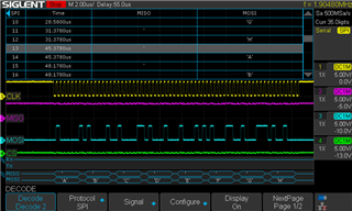
2. Why am I having so much difficulty triggering and decoding the 430 - 3 pin signal? I'm triggering on CLK falling edge. Same results for scope or LA. See scope image for a successful 3 pin master tx decode.

3. The 430 P8 also supports UART, SPI, and I2C, where I2C has two pull-ups on SDA & SCL - which are shared with UCB1SIMO & UCB1SOMI. UCB1 MOSI is working fine, I don't think the I2C pull-ups will cause a problem for SPI. Just pulls pin high by default, signal logic will go high or low as needed. Please confirm?
  • 1) In Slave mode, 4-pin works as you would expect, and is generally preferable to 3-pin. In Master mode, 4-pin doesn't work the way you (probably) expect [Ref UG (SLAU208Q) Fig 37-2], and you probably want to use 3-pin plus a GPIO for /CS (you can use the STE pin if you want). Which mode are you using?

    2) My first guess is something to do with clock phase, which I expect you also have to tell your Analyzer about. Keep in mind that UCCKPH is set opposite to CPHA.

    3) I expect this will work, and the pull-ups won't get in the way. I've seen these (usually weaker ones) used for both SPI and UART to keep pins from wiggling during reboots. You should make sure that only one of J4/J5 is connected to anything, since whatever is at the other end may drive one of the lines whether you want it or not.

    What's the difference between the Analyzer decode on the top and on the bottom? The bottom one seems happy enough.

  • Thanks for the reply.

    1 - Tried 4 pin master & slave modes & could not even get pulses to scope, I will try 3 pin with a GPIO CS. I prefer 4 pin as well.

    2 - The SPI port & scope or LA are set for the same SPI parameters. Did not know CPOL & CPHA should be opposite?

    3 - My drawing note says to use them separately - I appreciate the comment, not connected to anything beyond what you need to work at that time.

    The scope shot shows the only correct decode out of 10+ attempts on stop. When running continuously you see "ABC" fly by occasionally, but mostly ASCII gibberish. If you contract the time base to show more pulses, you can't see what the data values are at the bottom of the screen. You can scroll through the table on the top part of the screen to see what the data is.

  • 1) I recommend 3-pin (+GPIO for /CS) for the Master and 4-pin for the Slave. A Slave by itself won't produce any pulses, since the Master controls SCK. 

    2) UCCKPL should be set the same as CPOL. UCCKPH should be set opposite to CPHA.

  • My problem might be that I'm not setting UCCKPL or UCCKPH at all, just CPOL and CPHA. Where are the former set?

    Tried numerous permutations and 4 pin does not decode at all, 3 pin decodes correctly about 2 out of 10 attempts. When it works it correctly decodes about 3500 characters.

    Sample C code below for port setup function, and data string Tx function.

    3500 characters.

    // setup MSP430F5638 P8 UCB1 SPI
    // 4 pin master tx mode
    //      nothing works, no decode at all
    // 3 pin master tx mode
    //      tried with & without STE used as GPIO CS
    //      properly decodes about 2 out of 10 attempts
    //      the 2 that work each capture up to 3500 characters correctly for 10 ms @ 500 MHz LA
    //      8 fails get ASCII gibberish for all characters
    // uses polling, according to TI tech support, for high speed SPI, ISR's are slower, don't use them
    // P8 Tx string = "ABCDEFGH" to scope or LA, same results for both instruments
    void SPI_2_M_init(void)
    {
        UCB1CTL1 = 0x01;         // disable UCB1 during configuration
    
        // 4 pin SPI synch - no pulses at all
        // MSP430 does not work in 4 pin mode to LA's anyway
        // set all SPI-2 serial parameters
        // high nibble 1110 = clock phase = 1, polarity = 1, MSB first = 1, 8-bit = 0
        // low nibble 1101 = Master = 1, 4 pin STE low = 10, Synch Mode = 1
        // 7654 3210
        // 1110 1101 = 0xED
    //    UCB1CTL0 = 0xED;
    
        // 4 pin SPI asynch - no pulses at all
        // try asynchronous - still not triggering LA1010
        // 7654 3210
        // 1110 1100 = 0xEC
    //    UCB1CTL0 = 0xEC;
    
        // 3 pin SPI mode - trigger on Ch1 CLK - decodes 2 of 10 attempts
        // trigger on CS low does nothing, no decode at all
        // works 3 pin mode - CLK, MOSI pulses, MISO high, but no STE pulses
        // MSP430 only seems to like 3 pin mode
        // try 3 pin, sync - this triggers the LA1010 & U3Pro16
        // 1110
        // clock phase = 1, polarity = 1, MSB first = 1, 8-bit = 0
        // 1001
        // Master = 1, 3-pin SPI = 00, synchronous mode = 1
        // 7654 3210
        // 1110 1001 = 0xE9
        UCB1CTL0 = 0xE9;        // tried asynch 0xE8, no difference
        // try CPHA = 0
        // 7654 3210
        // 0110 1001 = 0x69
    //    UCB1CTL0 = 0x69;        // never gets ABCD...
    
        // 7654 3210
        // 1000 0001 = 0x81
        // SMCLK = 10, Don't care xxxxx, software reset = 1
        UCB1CTL1 = 0x81;
    
        // BRW = divisor
        // tested BRW = 2 to 64, must be >= 6 when using X2 @ 24 MHz MSP430 clock
        UCB1BRW = 7;                      // X2 = 20 MHz / 7 = ~3 MHz (must be >= 6 to work)
    
        UCB1CTL1 &= ~0x01;       // enable UCB1 for use after configuration
    }
    
    // 8/27/24 - M Tx 3 pin, use GPIO to set / clear CS
    // Master Tx
    // uses polling
    // SPI-2 uses P8 UCB1
    // str = transmitted string
    void setup_430_P8_SPI_2_M_TX(unsigned char *str)
    {
        int i=0, length;
        length = strlen(str);
    
        // set alternate function for P8.4, P8.5, P8.6 - UCB1 SPI-2
        // leave P8.1 UCB1STE as GPIO to set / clear CS
        // 7654 3210
        // 0111 0000 = 0x70
        P8SEL |= 0x70;          // set for 3 pin mode
        // 7654 3210
        // 0111 0010 = 0x72
    //    P8SEL |= 0x72;        // set for 4 pin mode
    
        // set UCB1STE P8.1 for GPIO CS
        P8DIR |= BIT1;      // set UCB1STE to out, don't need, default
        P8OUT |= BIT1;      // set UCB1STE high
    
        // loop continuously
        // STE CS set high by default
        while(1)
        {
            P8OUT |= BIT1;      // set UCB1STE CS high
            // Tx the string
            for (i = 0; i < length; i++)
            {
                P8OUT &= ~BIT1;     // clear UCB1STE CS low to trigger on
                while(!(UCB1IFG & UCTXIFG))     // wait for transmit buffer empty
                    ;
                UCB1TXBUF = str[i];       // transmit a character
                //delayMs(10);
            }
            P8OUT |= BIT1;      // set UCB1STE CS high
        }
    }


    I've added a code file with my SPI setup function, and the Tx function.

  • My problem might be that I'm not setting UCCKPL or UCCKPH at all, just CPOL and CPHA.

    Using the provided defined symbols makes things a bit clearer:

        UCB1CTL0 = 0xE9;        
        // vs.
        UCB1CTL0 = UCCKPH | UCCKPL | UCMSB | UCMST | UCSYNC


    The naming of CPOL CPHA etc. is always confusing to me so I consult the data sheets to find out what is expected. Which works most of the time although not always. A little OLED display have me trouble because the data sheet seemed to indicate it didn't care about the idle state of the clock. It did.

**Attention** This is a public forum