This thread has been locked.

If you have a related question, please click the "Ask a related question" button in the top right corner. The newly created question will be automatically linked to this question.

MSP430F2617: PWM output with 4ms delay issues

Part Number: MSP430F2617
Other Parts Discussed in Thread: DRV8955

Tool/software:

Hello,

I will do my best to explain my end goal, but I may not be explaining it quite correctly so bear with me. 

I am attempting to generate, using one singular pin on the MSP430, a "delayed" PWM signal where the signal begins HIGH (3.3V) for 4ms and then begins to pulse based on my desired frequency and duty cycle. This will be generated based on a GPIO input that comes from an external source.

My approach to this has been:

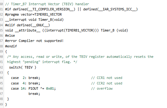
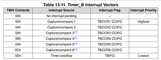
1) Setup Timer B (corresponding to P4.3)

- Setup CCR0 and CCR3 in UP (MC_1) mode

- Initialize their interrupts by ORing the compare/control register with CCIE

- Initialize the corresponding pin to a GPIO pin initially

2) Setup Timer A (only using this Timer to count to 4ms)

- Setup CCR0 to hold a value of 32000, @8MHz DCOCLK this should be equal to 4ms

- Initialize the interrupt the same way as Timer B

3) Setup all the corresponding GPIO, in this case I am using P6.5 (yes, I know, I should have probably routed this signal to P1 or P2 so I can use a hardware interrupt, but I am trying to do this with software polling, that might be my problem as to why I cannot get this to work)

- Initialize P6.5 as a GPIO input that is a pull down

4) In my main, create an infinite loop using while(1), 

if(trigger_input) -> set P4.3 high using P4OUT |= BIT3 -> activate Timer A -> in Timer A IRQ, set P4.3 to a PWM pin using P4SEL |= BIT3 -> activate Timer B -> flip flop between IRQ for CCR0 and CCR3 in TB.

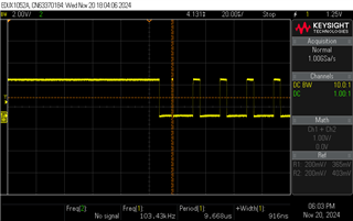
This does not seem to work, or, rather, it seems to work "sometimes".

To give a little bit more context: I am trying to use this PWM signal as an input to DRV8955, a motor driver chip that has 4 PWM inputs and 4 PWM outputs. For some reason, I cannot seem to see the initial GPIO pulse with the "delay" prior to the actual PWM itself on the output. Also - for whatever reason, my initial delay is only 1.5ms instead of 4ms and I'm not sure why. The code I am using to set my clock to 8MHz is the following:

DCOCTL = CALDCO_8MHZ; //Change DCO = MCLK = 8 MHz
BCSCTL1 = CALBC1_8MHZ | XTS; //Basic clock system control register

Any insight into how to properly do this would be great! I can post the entirety of my code as well to go over any nuances but I did not want to make this post too much of an essay.

Thank you in advance, this has been an issue I've been working on for almost two weeks now with no luck. 

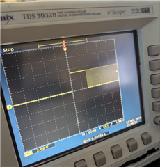
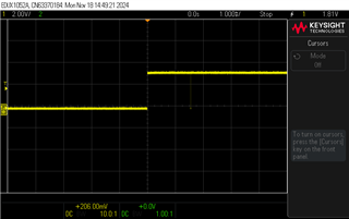
My desired waveform looks as follows:

  • Hi,

    if(trigger_input) -> set P4.3 high using P4OUT |= BIT3 -> activate Timer A -> in Timer A IRQ, set P4.3 to a PWM pin using P4SEL |= BIT3 -> activate Timer B -> flip flop between IRQ for CCR0 and CCR3 in TB.

    This procedure looks correct on my side. Can you show a waveform you are getting now? So we can know better of what part of the code failed. 

    I would be good to send your code here. I would also suggest to separate the delay function and the PWM function for test first. Since you could not get a correct 4ms pulses. You can disable the Timer B and only test the Timer A function. 

    Best regards,

    Cash Hao

  • Hi Cash,

    My reply is unfortunately later than I would have liked - I did not get a chance to test just Timer A.

    How would I go about doing this? My first attempt was to do as follows:

    #include <msp430.h> 
    #include "msp430f2617.h"
    #include <init.h> //Typically initPWM, initParams, and Initialize() are all in init.h
    
    //I omitted Initalize() because all it does is initialize all unused ports as outputs
    
    
    void initPWM()
    {
        // -- Interrupt Initialization -- //
        // TA = Counter
        // TB = PWM
        TA0CCTL0 |= CCIE;        // CCIE enables interrupts when initialized (CCRA0)
        //TA0CCTL2 |= CCIE;
        TB0CCTL0 |= CCIE;        // Period register for Timer B
        TB0CCTL3 |= CCIE;        // Duty cycle register for Timer B - P4.3
        //TA0CCTL2 &= ~CCIFG;
        TA0CCTL0 &= ~CCIFG;      // Clear interrupt flag when initialized
        TB0CCTL0 &= ~CCIFG;
        TB0CCTL3 &= ~CCIFG;
    
    
        __bis_SR_register(GIE);
    }
    
    void initParams()
    {
        WDTCTL = WDTPW | WDTHOLD;       //Stop Watch Dog Timer (WDT)
    
        DCOCTL = CALDCO_8MHZ;           //Change DCO = MCLK = 8 MHz
        BCSCTL1 = CALBC1_8MHZ | XTS;    //Basic clock system control register
        //BCSCTL2 = DIVS_0;


        // -- GPIO Initialization --
    
        //Status LED
        P6DIR |= BIT5;                  //P6.5: Micro status LED
        set_MCU_status_lo;
    
        //DRV Fault LED
        P1DIR |= BIT4;                  //P1.4: Fault LED
        clear_DRV_fault;
    
        //nSLEEP (DRV Sleep)
        P3DIR |= BIT4;                  //P3.4: nSLEEP
        sleep_DRV;
    
    
        //VREF (Output) is P6.6 / DAC0
        //Making it a standard GPIO Out for testing
        P6DIR |= BIT6;
        P6SEL &= BIT6;
        P6OUT |= BIT6;
    
        //24V TRIG IN
        P6DIR &= ~BIT4;                 //P6.4: MSP_TRIG_IN
        P6SEL &= ~BIT4;                 //GPIO mode
        P6REN |= BIT4;                  //resistor pull up/down enabled
        P6OUT &= ~BIT4;                 //pull down - this will keep the value of P6.4 LOW until a signal arrives
    
    
        // -- PWM Initialization -- (P4.1 - P4.3 are not used currently) //
    
    
        // We have two timers - P4.0 for driving and P2.2 for counting to 4ms //
    
        //P4.0, IN1 output
        P4DIR |= BIT0;                  //P4.0: IN1
        P4SEL &= ~BIT0;
        P4OUT &= ~BIT0;                 //Default to LOW
    
    
        //P4.1, IN2 output
        P4DIR |= BIT1;                  //P4.1: IN2
        P4SEL &= ~BIT1;
        P4OUT &= ~BIT1;                 //Default to LOW
    
    
        //P4.2, IN3 output
        P4DIR |= BIT2;                  //P4.2: IN3
        P4SEL &= ~BIT2;
        P4OUT &= ~BIT2;                 //Default to LOW
    
    
        //P4.3, IN4 output
        P4DIR |= BIT3;                  //P4.3: IN4
        P4SEL &= ~BIT3;                 //Makes it a GPIO pin
        P4OUT &= ~BIT3;                 //Default to LOW
    
    
        //P2.3, Timer used for counting to 4ms
        P2DIR |= BIT3;                  //Using this timer only for counting
        P2OUT &= ~BIT3;                 //Set to low initially
    
        // Active timer settings //
        //dT = N / fPWM; N is the count below, fPWM * dT = N -> 8MHz * (time_elapsed) = Period
    
        TB0CCR0 = 200;                          //Period
        TB0CCR3 = 50;                    //Duty cycle
        // 50 / 200 = 25 % Duty
    
        TA0CCR0 = 32000;                    //Period
        //TA0CCR2 = 0;                      //Duty cycle
        // Counts for 4ms @ 8MHz MCLK
    
        //Set the timer modes
        //TA0CCTL2 |= OUTMOD_7;
        TA0CCTL0 |= OUTMOD_7;            //PWM Mode - Set, should correspond to P2.2
        TB0CCTL3 |= OUTMOD_7;            //PWM Mode - Reset/set, should correspond to P4.0
    }


    int main(void) // V1.0.1 hardware
    {
    
        Initialize();   //Initialize the MSP430, in general, see init.c for more
        initParams();   //Set the parameters for our configuration
        initPWM();
    
        
        while(1)
        {
            //read_trig_in = P6IN & BIT4
            if(read_trig_in)
            {
                set_MCU_status_hi;  //Are we on? (LED on my board)
                
                set_IN4_gpio;       //Initial output (P4.3 output)
    
                set_IN4_hi; //Start the 4ms pulse
    
                TACTL |= MC_1 + TBSSEL_2 + ID_0;    //Enable timer A
    
                //TBCTL |= MC_1 + TBSSEL_2 + ID_0;
    
            }
    
            else if((P4OUT & BIT3) && read_trig_in)
            {
                //do nothing
                __no_operation();
                //continue;
            }
    
            // Exit if our trigger is not active
            else
            {
    
                set_IN4_gpio;   //Set back to GPIO mode
                set_IN4_lo;
                clear_timer_A;
                set_MCU_status_lo;
                initPWM(); 
            }
    
            //set_IN4_lo;
        }
    
    
    }
    
    // ISRs //
    
    
    // 4ms counter //
    #pragma vector = TIMER0_A0_VECTOR
    __interrupt void ISR_TA0_CCR0(void)
    {
        if(read_trig_in)
        {
    
            set_IN4_lo; //This ends the pulse and allows me to check timing
    
    
            TA0CCTL0 &= ~CCIFG;                  //clears interrupt flag for Timer A.0
    
            //stop_timer_A;   //Do I need this?
    
            TA0CCTL0 &= ~CCIE;
            
        }
        else
        {
            clear_timer_A;
        }
    
    }
    

    Apologies for the many lines of code, I believe a lot of these may be redundant. 

    It seems like setting up TA0CCR0 to count to 4ms is not working as expected here. Do you know the reason why? I think my understanding of the Timer blocks is a little bit flawed.

    This is the waveform I get on P4.3: 

  • "Output modes 2, 3, 6, and 7 are not useful for output unit 0 because EQUn = EQU0."

  • Ahhh, so CCR0 needs a different OUTMOD set in the CCTL it seems. I have been trying this with OUTMOD_1 for TA0CCTL0 as well, but am seeing the same waveform.

    The idea here is:
    1) Set the output high

    2) Start the timer

    3) During timer interrupt (after 4ms elapsed), bring output low

    That does not seem to be happening here. There is a small inverse pulse that occurs at approx. 1.5ms and I am not sure why.

    Do I even need to set an OUTMOD for just using a timer to count? I'm not using this specific pin attached to TA0CCR0.

  • Hi,

    When you debug your project, can your code hit the TA interrupt routine? 

    Because in the code I does not see you enable the GIE in the code, something like __bis_SR_register(LPM0_bits + GIE); 

    Best regards,

    Cash Hao

  • I moved the global interrupt to the beginning of main, previously it was in initPWM().

    I am able to hit the TA0 and TA1 interrupts and I am using them to begin and end the 4ms pulse. It seems to be working, but only on the first cycle from a fresh reboot. Can you take a look and see if you can tell why it's only able to run once? I can't seem to figure this one out. I think it has something to do with the interrupt enables in CCTL registers.

    The variable aDone here is used to denote when the 4ms pulse has ended so that I can only have it happen once per external trigger input. I modified the while loop slightly: 

        while(1)
        {
            //sleep_DRV;
            // Do stuff only if our trigger is active
            if(read_trig_in && (aDone == 0))
            {
                set_MCU_status_hi;  //Are we on?
    
                TACTL |= MC_1 + TASSEL_2 + ID_0 ;    //activates Timer A?
            }
    
            else if(read_trig_in && (aDone))
            {
                //do nothing
                if(aDone)
                    set_IN4_pwm;
    
                set_MCU_status_lo;
                //continue;
            }
    
            // Exit if our trigger is not active
            else
            {
    
                sleep_DRV;  //Sleep the motor driver
                set_IN4_gpio;   //Set back to GPIO mode
                set_IN4_lo;
                clear_timer_A;
                clear_timer_B;
                //__delay_cycles(1000000);
                //clear_DRV_fault;
                set_MCU_status_lo;
                aDone = 0;
                initPWM();
            }
        }

    Here are the working ISRs:

    #pragma vector = TIMER0_A0_VECTOR
    __interrupt void ISR_TA0_CCR0(void)
    {
        if(read_trig_in)
        {
    
            set_IN4_lo;
            
    
            //stop_timer_A;   //Do I need this?
    
            TB0CTL |= MC_1 + TBSSEL_2 + ID_0;    //idk
            TA0CCTL0 &= ~CCIFG;                  //clears interrupt flag for Timer A.0
    
    
            TA0CCTL0 &= ~CCIE;
            aDone = 1;
        }
        else
        {
            clear_timer_A;
            set_IN4_gpio;
            aDone = 0;
        }
    
    }
    
    #pragma vector = TIMER0_A1_VECTOR
    __interrupt void ISR_TA0_CCR2(void)
    {
        if(read_trig_in)
        {
            set_IN4_hi;
            TA0CCTL2 &= ~CCIFG;
    
            TA0CCTL2 &= ~CCIE;
        }
        else
        {
            set_IN4_gpio;
            clear_timer_A;
            aDone = 0;
        }
    }

    Thanks,

    Sam

  • Hi,

    Emm, only run once. May be you can try directly use '=' instead of '|=' to assign values ​​to registers.

    For example, TB0CTL = MC_1 + TBSSEL_2 + ID_0;

    Best regards,

    Cash Hao

  • That did not change anything, unfortunately. There has to be some flag or something I am not resetting properly after aDone gets set and I cannot determine what that is. I believed it was due to disabling CCIE but it seems as though when I re-enable it in the else{} statement of the while loop, it does not seem to change the behavior, so it must be something else I'm not clearing.

    I assume this is not a matter of needing to clear TAIFG?

  • I added in @ line 14, an additional clearing of the CCR3 interrupt:

    #pragma vector = TIMER0_B1_VECTOR
    __interrupt void ISR_TB0_CCR3(void)
    {
        if(read_trig_in)
        {
            TB0CCTL3 &= ~CCIFG; //Clear the interrupt flag
        }
        else
        {
            clear_timer_B;
            set_IN4_gpio;
            set_IN4_lo;
            sleep_DRV;
            TB0CCTL3 &= ~CCIFG; //Clear the interrupt flag
        }
    }

    Timer A is consistently lasting 4ms now, great!

    One outstanding issue I have still with this:

    Occasionally, after the TimerA interrupt has cleared, I will get this ~900ns pulse before the PWM starts. This is intermittent and does not happen every time. I genuinely cannot tell if this is due to a timing issue involving TimerA or if this is completely a TimerB issue.

    I assume that this has to do with how I am software polling for the trigger input, however, I believe this might also be solvable within the ISRs. This feels like another case of not clearing a flag at the correct time, thus causing this small blip to occur.

    I tried an assortment of combinations of clearing CCIFG in my else() for each of the ISRs and was not able to get anymore info on this. 

  • Hi,

    What is the purpose of this timerB interrupt routine? If you only need to output the PWM, there is no need to use its interrupt to do it. 

    Best regards,

    Cash Hao

  • How would I generate PWM without using timer interrupts? I'm not sure I understand. I thought the entire point was to set up whichever CCRx register corresponds to a pin on the MCU and depending on the OUTMOD will determine how the pin will change based on whenever CCRx and CCR0 fire an interrupt.

    Is my understanding incorrect?

  • Hi,

    Well, for output an PWM waveform does not require changing the GPIO pin status in the interrupt routine manually. Below is an example code how to generate PWM waveform using timerA. It does not require interrupt routine to output the PWM signal. 

    https://dev.ti.com/tirex/explore/node?node=A__AD7Nu6Gz3Yuq.n7HkyOW1g__msp430ware__IOGqZri__LATEST

    Best regards,

    Cash Hao

  • Hi Cash,

    Correct, I am doing that with TimerB for PWM. I am only manually setting the GPIO pin high in TimerA ISR so that I can have a pulse. I felt this way was easier than trying to change duty cycle in between interrupts. Do you suggest I do it a different way?

    There are also other GPIO I need to manage at the end of the TimerB interrupts. Also, I believe you need to clear CCIFG in each interrupt to exit the interrupt, no?

  • Hi,

    Correct, I am doing that with TimerB for PWM. I am only manually setting the GPIO pin high in TimerA ISR so that I can have a pulse. I felt this way was easier than trying to change duty cycle in between interrupts. Do you suggest I do it a different way?

    It is okay to use TimerA ISR to generate a pulse. However, if you do need these ISRs in your code. I would suggest you to write ISR in below way. You will check the TBIV/TAIV first and know what interrupt is happening here. And add for application code under certain case.  You can find the definition for each case in device UG TBIV/TAIV Register.  Also, any access, read or write to the TBIV/TAIV register will automatically reset the highest pending interrupt flag. You will not need to clear each interrupt's CCIFG by this way. 

    Best regards,

    Cash Hao

  • Would you mind giving me a slightly more specific example to my use case?

    Would I have four separate ISRs (TimerB0, TimerB1, TimerA0, TimerA1 vectors) and use a switch statement for the respective Interrupt Vector register?
    For example: TimerB ISRs will switch on TBIV and TimerA will switch on TAIV. 

    I'm not familiar with the behavior of TAIV, I was a bit confused based on the data sheet. 

    It would be very helpful if you can explain more specifically what you mean. I have not seen any examples like this before.

  • Hi,

    Okay, For example, take your code as below. 

    #pragma vector = TIMER0_B1_VECTOR
    __interrupt void ISR_TB0_CCR3(void)
    {
        if(read_trig_in)
        {
            TB0CCTL3 &= ~CCIFG; //Clear the interrupt flag
        }
        else
        {
            clear_timer_B;
            set_IN4_gpio;
            set_IN4_lo;
            sleep_DRV;
            TB0CCTL3 &= ~CCIFG; //Clear the interrupt flag
        }
    }

    It could be change to below one. 

    #pragma vector = TIMER0_B1_VECTOR
    __interrupt void Timer_B(void)
    {
    
        switch( TBIV )
       {
         case  2: break;                          // CCR1 not used
         case  4: break;                          // CCR2 not used
         case  6:                                 // CCR3 CCIFG
             if(!read_trig_in)
             {
                 clear_timer_B;
                 set_IN4_gpio;
                 set_IN4_lo;
                 sleep_DRV;
             }
             break;
         case 14: break;                 // overflow
       }
    
    }

    For each interrupt source in TBIV, You can find the definition in UG table 13-11

    I hope this example can help you understand how it works.

    Best regards,

    Cash Hao

  • Thank you for your help, Cash. So far it seems that my code works as is, but I would like to clean it up and improve it by using your strategy. It seems to be more clear and less error prone. Your solution is probably also faster than if, else statements.

    Since this thread is long enough, I'll mark it as resolved and create a new thread if I need to revisit this in the future.

**Attention** This is a public forum