This thread has been locked.

If you have a related question, please click the "Ask a related question" button in the top right corner. The newly created question will be automatically linked to this question.

MSP430FR6047:  MSP430FR6047:When the TIDA-01486 was EVM430FR6047 connected, the ADC did not capture the correct waveform very well

Part Number: MSP430FR6047
Other Parts Discussed in Thread: TIDA-01486, THS3095

Tool/software:

Hi everyone, I need to use the V-clamp mounting method on PVC piping and metal piping, but I found that the reception signal is a bit weak, and I was recommended the TIDA-01486.TIDA-01486 reference design | TI.com

After connecting TIDA-01486, do I need any additional configuration to perform ADC acquisition?I have removed the capacitors and resistors connected to the signal pins on the EVM board as required, and connected them correctly to the signal amplifier circuit.The circuit diagram is as follows:
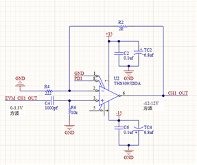
When testing in the lab, I only used one measurement loop, that is, from EVM_CH0_OUT to EVM_CH1_IN.And on the oscilloscope I am sure I see a nice waveform.

The green signal is the amplified drive signal, which is CH0_OUT in the schematic diagram, and the yellow signal is the amplified receiving signal, which is EVM_CH1_IN.

You can see that the amplitude is about 150mv and the time difference is about 80us, I'm not sure if the signal strength can measure the flow properly, but I can't see the waveform at all on the upper computer.

I don't know why this is happening, please help me.The configuration parameters of the EVM are as follows.

  • Hi,

    First, the transmit signal does not look correct. The R6 in the reference should be 1k Ohm instead of 10k. 

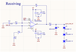
    And for the receiving path, the circuit seems weird too. The R18, R20 is not correct, there should be a Vbias here. And the R14 should be 10 Ohm. 

    For more information, please refer to this post. We have solved several issues using TIDA-01486 in that post. And it may help you in your design. 

    https://e2e.ti.com/support/microcontrollers/msp-low-power-microcontrollers-group/msp430/f/msp-low-power-microcontroller-forum/1421962/evm430-fr6047-cannot-get-the-tida-01486-amplifier-board-working/5519083#5519083

    Best regards,

    Cash Hao

  • Hi,Cash.

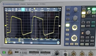
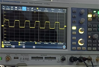
    For the drive path, when I set R6 to 1K, there is a noticeable shift in the square wave signal. I thought it was an RC filter circuit, so I modified the resistance value of the resistor. The left image shows the waveform before the modification, and the right image shows the modified waveform.

    For the receive circuit, I may have made the wrong modification.
    I noticed this post and I think his problem is similar to mine, I also had a heating issue with the op amp chip and the current was abnormal, and when I isolated the drive path from the receive path on the circuit, the problem was solved.

    I will read it in detail and try to modify my circuit.

    Your reply was very helpful to me, thank you and I will spend a few days modifying my circuit.

  • Hi,

    The left figure should be the correct one. The exciation signal is supposed to be -15V to +15V. 

    Best regards,

    Cash Hao

  • Hi,Cash.
    I've changed my circuit exactly to the reference design and added resistors and capacitors at the connection to the EVM board as shown below,The amplifier now has an amplification of 2.


    It's worth noting that I only have one pair of transducers in my design, so I removed the multiplexer THS3095, which means that the single transmit path is now.
    EVM_CH0_OUT --> CH0_OUT --> transducer CH0
    Transducer CH1-->CH1_IN-->EVM_CH1_IN
    The other way is the same.

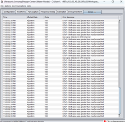
    And, I got some data on the OP and the algorithm seems to be able to do the calculations, but it doesn't work very well.

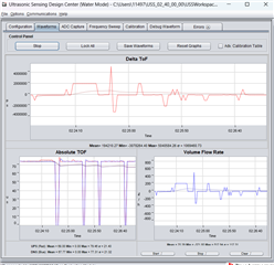
    From the OP, it seems that the problem is only with signal strength and stability. But on the oscilloscope, I can't see any reflected waveforms, and I don't know which waveform of the ADC sampling signal is being received on the host computer.

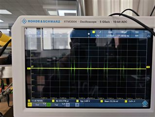
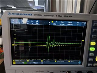
    The left side shows the waveform on a single transducer, which appears to have a set of periodic waveforms forming it, and the right side shows the amplified waveform of that waveform. In my understanding, there should appear to be a set of driving waveforms at each end of the transducer, and immediately following that, there would be a set of receiving waveforms. Like the last picture I posted.

    But strangely, the OP seems to capture the waveform normally which is similar to the standard waveform inside the reference design, so this makes me feel strange, can you explain to me what kind of waveform is required to calculate the flow rate in ti's algorithm.Is it the waveform on the left or the waveform on the right?

  • Hi,

    The ADC capture signal is a good start shows below. You can start with it and modify the parameters to get a better ADC capture result following this guide. https://dev.ti.com/tirex/explore/node?node=A__AUxLkAvzLrljvLBB0bSqSw__MSP430-ACADEMY__8HaEUeq__LATEST

    Best regards,

    Cash Hao

  • Hi,cash

    I tested it all day yesterday in the lab and got some info to share some of it with you.
    First, I tested a ±100mV waveform with an internal gain of 16.3db, which corresponds to an adc sampled waveform amplitude of about ±1000 codes. Does this mean that no matter what, I have to make sure that the amplitude of the accepted waveform can't be less than ±100mV, otherwise it will have an impact on the calculation, please confirm this.
    Secondly, the problem now is that in my test environment - external clamp v-mount on stainless steel tube, when the drive waveform is 0-3.3V,even after 2x amplification, the receive waveform is only about ±30mV,which is almost drowned in noise. I can't make accurate measurements.
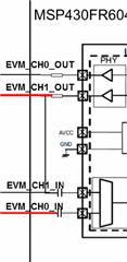
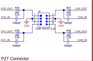
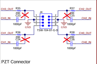
    So now the problem becomes I want to increase my drive voltage and the strength of the received signal, but in TIDA-01486, when linking the transducer, the output pin of the drive circuit is connected to the input pin of the receive circuit through a capacitor and a resistor, like below.

    However, if the amplification is 10x, then the chip pins of the receiver circuit will not be able to withstand the drive waveform generated by the driver circuit, as encountered in this link.https://e2e.ti.com/support/microcontrollers/msp-low-power-microcontrollers-group/msp430/f/msp-low-power-microcontroller-forum/1421962/evm430-fr6047-cannot-get-the-tida-01486-amplifier-board-working/5519083#5519083

    This seems to be a contradictory loop, do you think it would be possible to include a multiplexer between the driver and receiver circuits of the TIDA-01486, which could be used to isolate the two circuits and prevent them from affecting each other.

    I'm just posting the question on the forum first, but you can do so without having to respond to me in a timely manner, so have a great vacation. After that, any advice would be greatly appreciated!

  • Hi,

    Thanks for the consideration! have a happy holiday to you too. 

    1. Yes a good receive signal level is critical for you to get a valid TOF result. 

    2. No, this is a little misleading but the CHx_OUT and Chx_IN are not connected together. This can avoid your issue. 

    Best regards,

    Cash Hao

  • Hi,Cash

    I'm glad you got back to me.

    But sorry, for this picture, can you make it a little more clear why CHx_OUT and Chx_IN are not connected together.

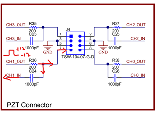
    In my understanding, in the TIDA-01486, for example, the ±12V square wave signal starts from CH1_OUT, passes through R36, to J4 to drive the transducer, but also passes through C24 to reach CH1_IN, and thus will be amplified by the op-amp chip, like the following figure.I saw this on the oscilloscope as well.

  • Hi,

    Oh sorry, I misunderstanding in the former post. I was wrong on that reply please ignore it. 

    You are correct in here. This issue can be avoid by controlling the enable pin PD1 on the receive opamp. And you can disable the amplifier while there is excitation signal firing. 

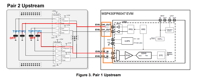
    One other thing is that the CH1_R will pass through a cap and then goes into the MCU USS input pin. Please do not forget it. Please refer to the cap and resister shows in below picture. 

    And actually my vocation starts from next week, and I will be out of office for a long time. 

    Best regards,

    Cash Hao

  • Hi,cash

    I'm glad you got back to me, I'm going to verify this with a new version of hardware, and have a great holiday season!

  • Thanks. I am going to close this thread first. There is a policy need to follow.

    Best regards,

    Cash Hao

**Attention** This is a public forum