This thread has been locked.

If you have a related question, please click the "Ask a related question" button in the top right corner. The newly created question will be automatically linked to this question.

MSP430FR2475: DCO calibration

Part Number: MSP430FR2475


Tool/software:

I'm trying to sort out the DCO-FLL configuration/calibration.  I read through UG, datasheet and MSP430FR2xx/FR4xx DCO+FLL Applications Guide. 

I still don't have all of it straight.  Please indicate below where I'm right and where I'm wrong.  That will help me make it through!

From User's Guide:

I assume the values below (from datasheet) map right into CSCTL0 register.  16-bit for 16-bit, that would fit.  Right?

However, according to DCOFTRIM bits description, they also play a role in the overall DCO calibration.  Right?

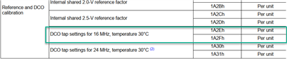
"Chip-specific trimmed", does that mean "each individual die"?  If so, I would expect these bits to be recorded in the Device Descriptor.  Are they part of 0x1A2E-0x1A30 or elsewhere or not accessible and automatically applied when DCOFTRIMEN=0?

One way or the other, I assume the tap settings from the Dev Desc is valid ONLY with default DCOFTRIM value or with DCOFTRIMEN=0... 

Regards

  • Hi Fred,

    Yes, the chip specific would mean each die gets it's own calibration values for those specified temps.  Let me get some clarification on these.

  • Any news?

  • Hi Fred,

    I do apologize for the delay in my response.  Ok, what is meant by "chip-specific trimmed" is referring to the process of adjusting or tuning the DCOTRIM values in software, which btw is mentioned in the user guide, section 3.2.11.2.  It is not referring to the values stored in the TLV memory.  Those values are loaded into the DCO at POR during the boot process.  Then later, in the application code you can perform your frequency specific tuning with the DCOTRIM bits.

    I copied the example code mentioned in the UG below for convenience.

    //******************************************************************************
    //  MSP430FR267x Demo - Configure MCLK for 1MHz operation, and REFO sourcing
    //                      FLLREF and ACLK. Use DCOFTRIM register to lock FLL.
    //
    //  Description: Configure MCLK for 1MHz. FLL reference clock is REFO.
    //               ACLK = default REFO ~32768Hz, SMCLK = MCLK = 1MHz.
    //               Use DCOFTRIM register to lock FLL. If FLL is locked and
    //               DCO tap is closest to 256, the DCOFTRIM value is the best one.
    //
    //                MSP430FR2676
    //         ---------------
    //     /|\|               |
    //      | |               |
    //      --|RST            |
    //        |          P1.0 |---> LED
    //        |               |
    //        |          P1.7 |---> SMCLK = 1MHz
    //        |               |
    //
    //   Longyu Fang
    //   Texas Instruments Inc.
    //   August 2018
    //   Built with IAR Embedded Workbench v7.12.1 & Code Composer Studio v8.1.0
    //******************************************************************************
    #include <msp430.h>
    
    void Software_Trim();                       // Software Trim to get the best DCOFTRIM value
    #define MCLK_FREQ_MHZ 1                     // MCLK = 1MHz
    
    int main(void) {
        WDTCTL = WDTPW | WDTHOLD;               // Stop watchdog timer
    
        __bis_SR_register(SCG0);                // Disable FLL
        CSCTL3 = SELREF__REFOCLK;               // Set REFO as FLL reference source
        CSCTL1 = DCOFTRIMEN_1 | DCOFTRIM0 | DCOFTRIM1 | DCORSEL_0;// DCOFTRIM=3, DCO Range = 1MHz
        CSCTL2 = FLLD_0 + 30;                   // DCODIV = 1MHz
        __delay_cycles(3);
        __bic_SR_register(SCG0);                // Enable FLL
        Software_Trim();                        // Software Trim to get the best DCOFTRIM value
        CSCTL4 = SELMS__DCOCLKDIV | SELA__REFOCLK; // set default REFO(~32768Hz) as ACLK source, ACLK = 32768Hz
                                                   // default DCODIV as MCLK and SMCLK source
    
        P1DIR |= BIT0 | BIT7;                   // set SMCLK and LED pin as output
        P1SEL1 |= BIT7;                         // set SMCLK P1.7 pin as second function
    
        PM5CTL0 &= ~LOCKLPM5;                   // Disable the GPIO power-on default high-impedance mode
                                                // to activate previously configured port settings
    
        while(1)                                // Toggle P1.0
        {
            P1OUT ^= BIT0;
            __delay_cycles(50000);
        }
    }
    
    void Software_Trim()
    {
        unsigned int oldDcoTap = 0xffff;
        unsigned int newDcoTap = 0xffff;
        unsigned int newDcoDelta = 0xffff;
        unsigned int bestDcoDelta = 0xffff;
        unsigned int csCtl0Copy = 0;
        unsigned int csCtl1Copy = 0;
        unsigned int csCtl0Read = 0;
        unsigned int csCtl1Read = 0;
        unsigned int dcoFreqTrim = 3;
        unsigned char endLoop = 0;
    
        do
        {
            CSCTL0 = 0x100;                         // DCO Tap = 256
            do
            {
                CSCTL7 &= ~DCOFFG;                  // Clear DCO fault flag
            }while (CSCTL7 & DCOFFG);               // Test DCO fault flag
    
            __delay_cycles((unsigned int)3000 * MCLK_FREQ_MHZ);// Wait FLL lock status (FLLUNLOCK) to be stable
                                                               // Suggest to wait 24 cycles of divided FLL reference clock
            while((CSCTL7 & (FLLUNLOCK0 | FLLUNLOCK1)) && ((CSCTL7 & DCOFFG) == 0));
    
            csCtl0Read = CSCTL0;                   // Read CSCTL0
            csCtl1Read = CSCTL1;                   // Read CSCTL1
    
            oldDcoTap = newDcoTap;                 // Record DCOTAP value of last time
            newDcoTap = csCtl0Read & 0x01ff;       // Get DCOTAP value of this time
            dcoFreqTrim = (csCtl1Read & 0x0070)>>4;// Get DCOFTRIM value
    
            if(newDcoTap < 256)                    // DCOTAP < 256
            {
                newDcoDelta = 256 - newDcoTap;     // Delta value between DCPTAP and 256
                if((oldDcoTap != 0xffff) && (oldDcoTap >= 256)) // DCOTAP cross 256
                    endLoop = 1;                   // Stop while loop
                else
                {
                    dcoFreqTrim--;
                    CSCTL1 = (csCtl1Read & (~DCOFTRIM)) | (dcoFreqTrim<<4);
                }
            }
            else                                   // DCOTAP >= 256
            {
                newDcoDelta = newDcoTap - 256;     // Delta value between DCPTAP and 256
                if(oldDcoTap < 256)                // DCOTAP cross 256
                    endLoop = 1;                   // Stop while loop
                else
                {
                    dcoFreqTrim++;
                    CSCTL1 = (csCtl1Read & (~DCOFTRIM)) | (dcoFreqTrim<<4);
                }
            }
    
            if(newDcoDelta < bestDcoDelta)         // Record DCOTAP closest to 256
            {
                csCtl0Copy = csCtl0Read;
                csCtl1Copy = csCtl1Read;
                bestDcoDelta = newDcoDelta;
            }
    
        }while(endLoop == 0);                      // Poll until endLoop == 1
    
        CSCTL0 = csCtl0Copy;                       // Reload locked DCOTAP
        CSCTL1 = csCtl1Copy;                       // Reload locked DCOFTRIM
        while(CSCTL7 & (FLLUNLOCK0 | FLLUNLOCK1)); // Poll until FLL is locked
    }
    

  • Dennis,

    Your code is very comprehensive.   With this I mind, I read again through documentation and got it all sorted out.

    I will assume DCSTL0.DCO accepts the 9 LSB from the two 8-bit TLV register, if we are to use it.

    Thank you very much for your support.

**Attention** This is a public forum