This thread has been locked.

If you have a related question, please click the "Ask a related question" button in the top right corner. The newly created question will be automatically linked to this question.

MSP430F6777A: Program and erase endurance interpretation

Part Number: MSP430F6777A

Tool/software:

Hello,

I am working with the MSP430F6777A and need to periodically store data in its flash memory every 15 minutes. The data must remain reliably stored for the next 10 years, which amounts to approximately 350,000 write cycles.

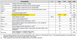
According to the datasheet, the minimum program/erase endurance is specified as 10,000 cycles, while the typical value is 100,000 cycles. The large difference between these values raises some concerns, and I need to determine how many flash sectors I should allocate to distribute the wear and achieve the required endurance.

My Questions:

  1. What is the reason for the 10× difference between the minimum and typical endurance values?
  2. Does the minimum value (10K cycles) represent extreme conditions (e.g., very low/high temperatures, low operating voltage), or can failures still occur around this limit even under ideal conditions (e.g., 3.3V operation at 25°C)?
  3. If I had 1 million MSP430F6777A chips running at 3.3V and 25°C, would some of them start failing after just 10,000 cycles at 3.3V and 25C? or are those failures only expected under harsher conditions?

Based on these factors, I am trying to determine whether allocating 4 sectors is sufficient to reach 350K cycles, or if I need 40 sectors to ensure long-term reliability.

Thank you for your insights!

Thanks.

  • Hi Mehmet,

    Your question has been received, and I need to confirm with the team about this issue, I will update it as soon as possible.

    Best Regards,
    Peter

  • Hello Peter,

    Any update here?

    Thanks.

  • Hi Mehmet,

    Sorry for the late reply. I've discussed with my team and also I found an application notes related to the issue.
    Understanding Typical and Maximum Program/Erase Performance

    To be honest, we currently haven't found any internal data reports regarding the erase endurance. In other words, as for the flash erase endurance testing of MCU, "10 thousand to 100 thousand erase cycles" is typically based on the original factory data experience value, rather than the result of the MCU manufacturer's own testing. The MCU manufacturer relies more on the data provided by the Flash original factory for design and verification, but in actual applications, the test results may vary depending on specific conditions.

    As mentioned in the file linked above, the minimum value (MIN) and typical value (TYP) in the flash erase endurance represent different types of statistical results.

    Minimum value is based on the worst-case test results, typically obtained under the most adverse conditions (such as high temperature, high voltage, etc.). The minimum value reflects the device's lowest endurance level under extreme conditions, while typical value is based on the average value of a large number of test data, typically obtained under standard conditions (such as 25°C, VCC=3.3V). The typical value reflects the device's average endurance level under normal operating conditions.

    For your actual application, if you have strict requirements for reliability and want to ensure that the device can still work normally under the worst-case conditions, it is recommended to refer to the minimum value for system design. Or if you are targeting most standard application scenarios, the typical value provides a more reasonable expected lifespan and can be referenced.

    Hope it will be helpful to you.

    Best Regards,
    Peter

  • How much data is written each time? If much less than the size of a segment then you can write multiple sets of data before having to erase.

**Attention** This is a public forum