


Tool/software:
New to embedded and I am just trying get LCD segments to light up on a slave unit to my master msp430.
I used example code from TI and inputted some code to represent my custom LCD screen.
UCB0 is UCB1 with how my pin setup is for my LCD.
Slave address is 0x7C and I want to try to use the APCTL command to light up all segments which would be C1111010. (im not sure what C represents.)
I've attached the address/ command byes here as well for reference.
I have pieces of what I need to do, I just am struggling on how to execute it. The i2c master writing code is on line 439.
My pseudo code example is
I2C_Master_WriteReg(SLAVE_ADDR, CMD_TYPE_0_MASTER, MasterType0, TYPE_0_LENGTH); // function w/ defines
I2C_Master_WriteReg(0x7C, "APCTL", ???, ???); // my defines filled in.
I2C_Master_WriteReg(0x7C, C1111010, MasterType0, TYPE_0_LENGTH); // alternative w/ defines filled in
What can I do to light up my LCD segments correctly and clear them when Im done?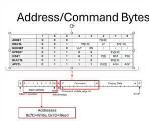
//******************************************************************************
//   MSP430F677xA Demo - USCI_B0, I2C Master multiple byte TX/RX
//
//   Description: I2C master communicates to I2C slave sending and receiving
//   3 different messages of different length. I2C master will enter LPM0 mode
//   while waiting for the messages to be sent/receiving using I2C interrupt.
//   ACLK = NA, MCLK = SMCLK = DCO 16MHz.
//
//                                     /|\ /|\
//                   MSP430F6779A      4.7k |
//                 -----------------    |  4.7k
//            /|\ |             P2.5|---+---|-- I2C Clock (UCB1SCL)
//             |  |                 |       |
//             ---|RST          P2.6|-------+-- I2C Data (UCB1SDA)
//                |                 |
//                |                 |
//                |                 |
//                |                 |
//                |                 |
//                |                 |
//
//   Nima Eskandari and Ryan Meredith
//   Texas Instruments Inc.
//   January 2018
//   Built with CCS V7.3
//******************************************************************************

#include <msp430.h>
#include <stdint.h>
#include <stdbool.h>

//******************************************************************************
// Pin Config ******************************************************************
//******************************************************************************

#define LED_OUT     P1OUT
#define LED_DIR     P1DIR
#define LED_PIN     BIT0

//******************************************************************************
// Example Commands ************************************************************
//******************************************************************************

#define SLAVE_ADDR  0x7C

/* CMD_TYPE_X_SLAVE are example commands the master sends to the slave.
 * The slave will send example SlaveTypeX buffers in response.
 *
 * CMD_TYPE_X_MASTER are example commands the master sends to the slave.
 * The slave will initialize itself to receive MasterTypeX example buffers.
 * */

#define CMD_TYPE_0_SLAVE      "APCTL"
#define CMD_TYPE_1_SLAVE      7
#define CMD_TYPE_2_SLAVE      1111010

#define CMD_TYPE_0_MASTER      "APCTL"
#define CMD_TYPE_1_MASTER      1111010
#define CMD_TYPE_2_MASTER      5

#define TYPE_0_LENGTH   1
#define TYPE_1_LENGTH   2
#define TYPE_2_LENGTH   6

#define MAX_BUFFER_SIZE     20

/* MasterTypeX are example buffers initialized in the master, they will be
 * sent by the master to the slave.
 * SlaveTypeX are example buffers initialized in the slave, they will be
 * sent by the slave to the master.
 * */

uint8_t MasterType2 [TYPE_2_LENGTH] = {'F', '4', '1', '9', '2', 'B'};
uint8_t MasterType1 [TYPE_1_LENGTH] = { 8, 9};
uint8_t MasterType0 [TYPE_0_LENGTH] = { 0};


uint8_t SlaveType2 [TYPE_2_LENGTH] = {0};
uint8_t SlaveType1 [TYPE_1_LENGTH] = {0};
uint8_t SlaveType0 [TYPE_0_LENGTH] = {0};

//******************************************************************************
// General I2C State Machine ***************************************************
//******************************************************************************

typedef enum I2C_ModeEnum{
    IDLE_MODE,
    NACK_MODE,
    TX_REG_ADDRESS_MODE,
    RX_REG_ADDRESS_MODE,
    TX_DATA_MODE,
    RX_DATA_MODE,
    SWITCH_TO_RX_MODE,
    SWITHC_TO_TX_MODE,
    TIMEOUT_MODE
} I2C_Mode;

/* Used to track the state of the software state machine*/
I2C_Mode MasterMode = IDLE_MODE;

/* The Register Address/Command to use*/
uint8_t TransmitRegAddr = 0;

/* ReceiveBuffer: Buffer used to receive data in the ISR
 * RXByteCtr: Number of bytes left to receive
 * ReceiveIndex: The index of the next byte to be received in ReceiveBuffer
 * TransmitBuffer: Buffer used to transmit data in the ISR
 * TXByteCtr: Number of bytes left to transfer
 * TransmitIndex: The index of the next byte to be transmitted in TransmitBuffer
 * */
uint8_t ReceiveBuffer[MAX_BUFFER_SIZE] = {0};
uint8_t RXByteCtr = 0;
uint8_t ReceiveIndex = 0;
uint8_t TransmitBuffer[MAX_BUFFER_SIZE] = {0};
uint8_t TXByteCtr = 0;
uint8_t TransmitIndex = 0;

/* I2C Write and Read Functions */

/* For slave device with dev_addr, writes the data specified in *reg_data
 *
 * dev_addr: The slave device address.
 *           Example: SLAVE_ADDR
 * reg_addr: The register or command to send to the slave.
 *           Example: CMD_TYPE_0_MASTER
 * *reg_data: The buffer to write
 *           Example: MasterType0
 * count: The length of *reg_data
 *           Example: TYPE_0_LENGTH
 *  */
I2C_Mode I2C_Master_WriteReg(uint8_t dev_addr, uint8_t reg_addr, uint8_t *reg_data, uint8_t count);

/* For slave device with dev_addr, read the data specified in slaves reg_addr.
 * The received data is available in ReceiveBuffer
 *
 * dev_addr: The slave device address.
 *           Example: SLAVE_ADDR
 * reg_addr: The register or command to send to the slave.
 *           Example: CMD_TYPE_0_SLAVE
 * count: The length of data to read
 *           Example: TYPE_0_LENGTH
 *  */
I2C_Mode I2C_Master_ReadReg(uint8_t dev_addr, uint8_t reg_addr, uint8_t count);
void CopyArray(uint8_t *source, uint8_t *dest, uint8_t count);

I2C_Mode I2C_Master_ReadReg(uint8_t dev_addr, uint8_t reg_addr, uint8_t count)
{
    /* Initialize state machine */
    MasterMode = TX_REG_ADDRESS_MODE;
    TransmitRegAddr = reg_addr;
    RXByteCtr = count;
    TXByteCtr = 0;
    ReceiveIndex = 0;
    TransmitIndex = 0;

    /* Initialize slave address and interrupts */
    UCB1I2CSA = dev_addr;
    UCB1IFG &= ~(UCTXIFG + UCRXIFG);       // Clear any pending interrupts
    UCB1IE &= ~UCRXIE;                       // Disable RX interrupt
    UCB1IE |= UCTXIE;                        // Enable TX interrupt

    UCB1CTL1 |= UCTR + UCTXSTT;             // I2C TX, start condition
    __bis_SR_register(LPM0_bits + GIE);              // Enter LPM0 w/ interrupts

    return MasterMode;

}


I2C_Mode I2C_Master_WriteReg(uint8_t dev_addr, uint8_t reg_addr, uint8_t *reg_data, uint8_t count)
{
    /* Initialize state machine */
    MasterMode = TX_REG_ADDRESS_MODE;
    TransmitRegAddr = reg_addr;

    //Copy register data to TransmitBuffer
    CopyArray(reg_data, TransmitBuffer, count);

    TXByteCtr = count;
    RXByteCtr = 0;
    ReceiveIndex = 0;
    TransmitIndex = 0;

    /* Initialize slave address and interrupts */
    UCB1I2CSA = dev_addr;
    UCB1IFG &= ~(UCTXIFG + UCRXIFG);       // Clear any pending interrupts
    UCB1IE &= ~UCRXIE;                       // Disable RX interrupt
    UCB1IE |= UCTXIE;                        // Enable TX interrupt

    UCB1CTL1 |= UCTR + UCTXSTT;             // I2C TX, start condition
    __bis_SR_register(LPM0_bits + GIE);              // Enter LPM0 w/ interrupts

    return MasterMode;
}

void CopyArray(uint8_t *source, uint8_t *dest, uint8_t count)
{
    uint8_t copyIndex = 0;
    for (copyIndex = 0; copyIndex < count; copyIndex++)
    {
        dest[copyIndex] = source[copyIndex];
    }
}

//******************************************************************************
// Device Initialization *******************************************************
//******************************************************************************

void initClockTo16MHz()
{
    UCSCTL3 |= SELREF_2;                      // Set DCO FLL reference = REFO
    UCSCTL4 |= SELA_2;                        // Set ACLK = REFO
    __bis_SR_register(SCG0);                  // Disable the FLL control loop
    UCSCTL0 = 0x0000;                         // Set lowest possible DCOx, MODx
    UCSCTL1 = DCORSEL_5;                      // Select DCO range 16MHz operation
    UCSCTL2 = FLLD_0 + 487;                   // Set DCO Multiplier for 16MHz
                                              // (N + 1) * FLLRef = Fdco
                                              // (487 + 1) * 32768 = 16MHz
                                              // Set FLL Div = fDCOCLK
    __bic_SR_register(SCG0);                  // Enable the FLL control loop

    // Worst-case settling time for the DCO when the DCO range bits have been
    // changed is n x 32 x 32 x f_MCLK / f_FLL_reference. See UCS chapter in 5xx
    // UG for optimization.
    // 32 x 32 x 16 MHz / 32,768 Hz = 500000 = MCLK cycles for DCO to settle
    __delay_cycles(500000);//
    // Loop until XT1,XT2 & DCO fault flag is cleared
    do
    {
        UCSCTL7 &= ~(XT2OFFG + XT1LFOFFG + DCOFFG); // Clear XT2,XT1,DCO fault flags
        SFRIFG1 &= ~OFIFG;                          // Clear fault flags
    }while (SFRIFG1&OFIFG);                         // Test oscillator fault flag
}

uint16_t setVCoreUp(uint8_t level){
    uint32_t PMMRIE_backup, SVSMHCTL_backup, SVSMLCTL_backup;

    //The code flow for increasing the Vcore has been altered to work around
    //the erratum FLASH37.
    //Please refer to the Errata sheet to know if a specific device is affected
    //DO NOT ALTER THIS FUNCTION

    //Open PMM registers for write access
    PMMCTL0_H = 0xA5;

    //Disable dedicated Interrupts
    //Backup all registers
    PMMRIE_backup = PMMRIE;
    PMMRIE &= ~(SVMHVLRPE | SVSHPE | SVMLVLRPE |
                SVSLPE | SVMHVLRIE | SVMHIE |
                SVSMHDLYIE | SVMLVLRIE | SVMLIE |
                SVSMLDLYIE
                );
    SVSMHCTL_backup = SVSMHCTL;
    SVSMLCTL_backup = SVSMLCTL;

    //Clear flags
    PMMIFG = 0;

    //Set SVM highside to new level and check if a VCore increase is possible
    SVSMHCTL = SVMHE | SVSHE | (SVSMHRRL0 * level);

    //Wait until SVM highside is settled
    while((PMMIFG & SVSMHDLYIFG) == 0)
    {
        ;
    }

    //Clear flag
    PMMIFG &= ~SVSMHDLYIFG;

    //Check if a VCore increase is possible
    if((PMMIFG & SVMHIFG) == SVMHIFG)
    {
        //-> Vcc is too low for a Vcore increase
        //recover the previous settings
        PMMIFG &= ~SVSMHDLYIFG;
        SVSMHCTL = SVSMHCTL_backup;

        //Wait until SVM highside is settled
        while((PMMIFG & SVSMHDLYIFG) == 0)
        {
            ;
        }

        //Clear all Flags
        PMMIFG &= ~(SVMHVLRIFG | SVMHIFG | SVSMHDLYIFG |
                     SVMLVLRIFG | SVMLIFG |
                     SVSMLDLYIFG
                     );

        //Restore PMM interrupt enable register
        PMMRIE = PMMRIE_backup;
        //Lock PMM registers for write access
        PMMCTL0_H = 0x00;
        //return: voltage not set
        return false;
    }

    //Set also SVS highside to new level
    //Vcc is high enough for a Vcore increase
    SVSMHCTL |= (SVSHRVL0 * level);

    //Wait until SVM highside is settled
    while((PMMIFG & SVSMHDLYIFG) == 0)
    {
        ;
    }

    //Clear flag
    PMMIFG &= ~SVSMHDLYIFG;

    //Set VCore to new level
    PMMCTL0_L = PMMCOREV0 * level;

    //Set SVM, SVS low side to new level
    SVSMLCTL = SVMLE | (SVSMLRRL0 * level) |
               SVSLE | (SVSLRVL0 * level);

    //Wait until SVM, SVS low side is settled
    while((PMMIFG & SVSMLDLYIFG) == 0)
    {
        ;
    }

    //Clear flag
    PMMIFG &= ~SVSMLDLYIFG;
    //SVS, SVM core and high side are now set to protect for the new core level

    //Restore Low side settings
    //Clear all other bits _except_ level settings
    SVSMLCTL &= (SVSLRVL0 + SVSLRVL1 + SVSMLRRL0 +
                 SVSMLRRL1 + SVSMLRRL2
                 );

    //Clear level settings in the backup register,keep all other bits
    SVSMLCTL_backup &=
        ~(SVSLRVL0 + SVSLRVL1 + SVSMLRRL0 + SVSMLRRL1 + SVSMLRRL2);

    //Restore low-side SVS monitor settings
    SVSMLCTL |= SVSMLCTL_backup;

    //Restore High side settings
    //Clear all other bits except level settings
    SVSMHCTL &= (SVSHRVL0 + SVSHRVL1 +
                 SVSMHRRL0 + SVSMHRRL1 +
                 SVSMHRRL2
                 );

    //Clear level settings in the backup register,keep all other bits
    SVSMHCTL_backup &=
        ~(SVSHRVL0 + SVSHRVL1 + SVSMHRRL0 + SVSMHRRL1 + SVSMHRRL2);

    //Restore backup
    SVSMHCTL |= SVSMHCTL_backup;

    //Wait until high side, low side settled
    while(((PMMIFG & SVSMLDLYIFG) == 0) &&
          ((PMMIFG & SVSMHDLYIFG) == 0))
    {
        ;
    }

    //Clear all Flags
    PMMIFG &= ~(SVMHVLRIFG | SVMHIFG | SVSMHDLYIFG |
                SVMLVLRIFG | SVMLIFG | SVSMLDLYIFG
                );

    //Restore PMM interrupt enable register
    PMMRIE = PMMRIE_backup;

    //Lock PMM registers for write access
    PMMCTL0_H = 0x00;

    return true;
}

bool increaseVCoreToLevel2()
{
    uint8_t level = 2;
    uint8_t actlevel;
    bool status = true;

    //Set Mask for Max. level
    level &= PMMCOREV_3;

    //Get actual VCore
    actlevel = PMMCTL0 & PMMCOREV_3;

    //step by step increase or decrease
    while((level != actlevel) && (status == true))
    {
        if(level > actlevel)
        {
            status = setVCoreUp(++actlevel);
        }
    }

    return (status);
}

void initGPIO()
{
    //LEDs
    LED_OUT &= ~LED_PIN; // P1 setup for LED & reset output
    LED_DIR |= LED_PIN;

    //I2C Pins
    P2SEL0 |= BIT5 | BIT6;      // Set P2.5,P2.6 to UCB1SCL, UCB1SDA
}

void initI2C()
{
    // Setup eUSCI_B0
    UCB1CTLW0 |= UCSWRST;                             // Enable SW reset
    UCB1CTLW0 |= UCMST | UCMODE_3 | UCSYNC | UCSSEL_2;// I2C Master, use SMCLK

    UCB1BRW_L = 160;                                  // fSCL = SMCLK/160 = ~100kHz
    UCB1BRW_H = 0;
    UCB1I2CSA = SLAVE_ADDR;                           // Slave Address is 048h
    UCB1CTLW0 &= ~UCSWRST;                            // Clear SW reset, resume operation
    UCB1IE |= UCNACKIE;
}

//******************************************************************************
// Main ************************************************************************
// Send and receive three messages containing the example commands *************
//******************************************************************************

int main(void) {

    WDTCTL = WDTPW | WDTHOLD;                 // Stop watchdog timer

    increaseVCoreToLevel2();
    initClockTo16MHz();
    initGPIO();
    initI2C();

    I2C_Master_WriteReg(SLAVE_ADDR, CMD_TYPE_0_MASTER, MasterType0, TYPE_0_LENGTH);
    I2C_Master_WriteReg(SLAVE_ADDR, CMD_TYPE_1_MASTER, MasterType1, TYPE_1_LENGTH);
    I2C_Master_WriteReg(SLAVE_ADDR, CMD_TYPE_2_MASTER, MasterType2, TYPE_2_LENGTH);

    I2C_Master_ReadReg(SLAVE_ADDR, CMD_TYPE_0_SLAVE, TYPE_0_LENGTH);
    CopyArray(ReceiveBuffer, SlaveType0, TYPE_0_LENGTH);

    I2C_Master_ReadReg(SLAVE_ADDR, CMD_TYPE_1_SLAVE, TYPE_1_LENGTH);
    CopyArray(ReceiveBuffer, SlaveType1, TYPE_1_LENGTH);

    I2C_Master_ReadReg(SLAVE_ADDR, CMD_TYPE_2_SLAVE, TYPE_2_LENGTH);
    CopyArray(ReceiveBuffer, SlaveType2, TYPE_2_LENGTH);

    __bis_SR_register(LPM0_bits + GIE);
    return 0;
}

//******************************************************************************
// I2C Interrupt ***************************************************************
//******************************************************************************

#if defined(__TI_COMPILER_VERSION__) || defined(__IAR_SYSTEMS_ICC__)
#pragma vector = USCI_B0_VECTOR
__interrupt void USCI_B0_ISR(void)
#elif defined(__GNUC__)
void __attribute__ ((interrupt(USCI_B0_VECTOR))) USCI_B0_ISR (void)
#else
#error Compiler not supported!
#endif
{
  //Must read from UCB1RXBUF
  uint8_t rx_val = 0;
  switch(__even_in_range(UCB1IV, USCI_I2C_UCBIT9IFG))
  {
    case USCI_NONE:          break;         // Vector 0: No interrupts
    case USCI_I2C_UCALIFG:   break;         // Vector 2: ALIFG
    case USCI_I2C_UCNACKIFG:                // Vector 4: NACKIFG
      break;
    case USCI_I2C_UCSTTIFG:  break;         // Vector 6: STTIFG
    case USCI_I2C_UCSTPIFG:  break;         // Vector 8: STPIFG
    case USCI_I2C_UCRXIFG3:  break;         // Vector 10: RXIFG3
    case USCI_I2C_UCTXIFG3:  break;         // Vector 12: TXIFG3
    case USCI_I2C_UCRXIFG2:  break;         // Vector 14: RXIFG2
    case USCI_I2C_UCTXIFG2:  break;         // Vector 16: TXIFG2
    case USCI_I2C_UCRXIFG1:  break;         // Vector 18: RXIFG1
    case USCI_I2C_UCTXIFG1:  break;         // Vector 20: TXIFG1
    case USCI_I2C_UCRXIFG0:                 // Vector 22: RXIFG0
        rx_val = UCB1RXBUF;
        if (RXByteCtr)
        {
          ReceiveBuffer[ReceiveIndex++] = rx_val;
          RXByteCtr--;
        }

        if (RXByteCtr == 1)
        {
          UCB1CTLW0 |= UCTXSTP;
        }
        else if (RXByteCtr == 0)
        {
          UCB1IE &= ~UCRXIE;
          MasterMode = IDLE_MODE;
          __bic_SR_register_on_exit(CPUOFF);      // Exit LPM0
        }
        break;
    case USCI_I2C_UCTXIFG0:                 // Vector 24: TXIFG0
        switch (MasterMode)
        {
          case TX_REG_ADDRESS_MODE:
              UCB1TXBUF = TransmitRegAddr;
              if (RXByteCtr)
                  MasterMode = SWITCH_TO_RX_MODE;   // Need to start receiving now
              else
                  MasterMode = TX_DATA_MODE;        // Continue to transmision with the data in Transmit Buffer
              break;

          case SWITCH_TO_RX_MODE:
              UCB1IE |= UCRXIE;              // Enable RX interrupt
              UCB1IE &= ~UCTXIE;             // Disable TX interrupt
              UCB1CTLW0 &= ~UCTR;            // Switch to receiver
              MasterMode = RX_DATA_MODE;    // State state is to receive data
              UCB1CTLW0 |= UCTXSTT;          // Send repeated start
              if (RXByteCtr == 1)
              {
                  //Must send stop since this is the N-1 byte
                  while((UCB1CTLW0 & UCTXSTT));
                  UCB1CTLW0 |= UCTXSTP;      // Send stop condition
              }
              break;

          case TX_DATA_MODE:
              if (TXByteCtr)
              {
                  UCB1TXBUF = TransmitBuffer[TransmitIndex++];
                  TXByteCtr--;
              }
              else
              {
                  //Done with transmission
                  UCB1CTLW0 |= UCTXSTP;     // Send stop condition
                  MasterMode = IDLE_MODE;
                  UCB1IE &= ~UCTXIE;                       // disable TX interrupt
                  __bic_SR_register_on_exit(CPUOFF);      // Exit LPM0
              }
              break;

          default:
              __no_operation();
              break;
        }
        break;
    default: break;
  }
}

