This thread has been locked.

If you have a related question, please click the "Ask a related question" button in the top right corner. The newly created question will be automatically linked to this question.

MSP430FR2355: MSP430 Flash has encountered an issue where it cannot be written (starting from address 0x1800)

Part Number: MSP430FR2355
Other Parts Discussed in Thread: UNIFLASH

Tool/software:

      After selecting 'erase protected information memory' in the uniflash download software, you can write it once, but it doesn't work after finishing. Then repeat it a few times, even if you erase it now, you won't be able to operate it anymore。

  • Hi huangjian,

    Could you clarify a few things for me:

    1. What do you mean by being able to write to it once but it doesn't work after finishing? Do you mean you can write to memory? Do you mean programming the device? Does the device no longer function as intended? Does the device turn on?
    2. Are you able to successfully erase the device? Are there any error messages?
    3. If the device doesn't seem to run, are you disabling the write protection for the information memory region before attempting to write?
    4. Is this issue happening within Uniflash or through attempting to program the device? Include any error messages that may appear (if applicable).

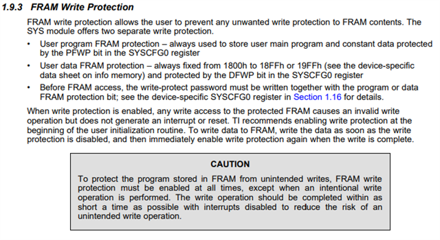
    I would suggest also referring to this section of the MSP430FR4xx and MSP430FR2xx family user's guide:

    Best,

    Owen

  • 1. After the uniflash erase, the simulator or programming can only be used to write once, and the second write attempt will fail.
    2. The chip can be erased normally through the simulator without error message
    3. Other functions of the chip are normal. The IO is set to high and set to low. Except for the operation of 0x1800FRAM, the write protection has been turned off.
    4. There is no special error message, only data writing fails, and data writing on a good chip is successful.
    At present, it is found that 6 PCSs fail to write data. This project has produced thousands of pieces in mass.

  • Hi huangjian,

    1. Can you please share how you are attempting to write to memory, such as the exact steps to replicate this issue?
    2. Can you please provide what you are attempting to write to that region of memory and what it looks like before and after flashing for the first time?
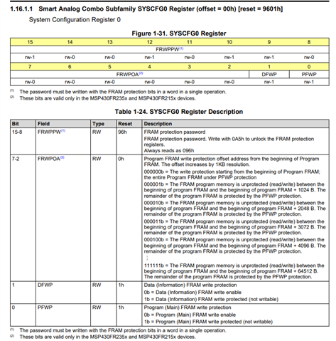
    3. What are the contents of the SYSCFG0 register? See below:

    Best,

    Owen

  • This is the CCS software and 430debug simulator used,Figure 1 shows the operation code. Video 1-2 is normal and video 3 is abnormal.

  • hi huangjian,

    Thanks for sharing the videos and code snippet. If possible, could you provide the full project so I can review the code?

    Best,

    Owen

  • Posting a picture of a display with your code is much less useful than actually posting the code. Takes more effort too.

    But this line bugs me in so many ways:

    SYSCFG0 = UPG_AREA(add) ? FWPW|DFWP : INF_AREA(add) ? FWPW|PFWP : FWPW|DFWP|PFWP;

    First is the undefined widgets UPG_AREA() and INF_AREA(). Functions? Macros? Do nothing?

    Then there is the convoluted use of the C conditional operator. Ugh.

    Finally, where is the write that fails?

  • Hi,Owen,We cannot provide full project,very sorry.

    Can you analysis the fail scene in the videro fiirst? 

  • We cannot find errors when we write data to FRAM,we will find data error by reading data back.

  • Hi xianyong,

    Without any context to the video, there's no way for me to understand how your code is written and intended to execute. The only thing I'm seeing in the video is that instead of reading or writing 16 bits, you're reading or writing 24 bits.

    You mentioned that you don't find errors when you write to FRAM, but how do you know this? Can you confirm that the data you want written to FRAM is actually being written? It seems like the data may not be written to FRAM. Could be an issue with protection.

    If there's any further information you can provide, such as more code snippets or an in-detail explanation of what you're doing, I may be able to assist you.

    Best,

    Owen

  • Hi,Owen,Thanks for you reply,The errors shown in the video are not caused by the code.There have many ways to operate FRAM address 0x1800,We used 430debugger to debug it in the video,not by our code.So,We can analysis the fail scene in the video fiirst.

    In the video,we can change data on a good chip but cannot change it on a failed chip.

    As for you doubt about "Can you confirm that the data you want written to FRAM is actually being written?" ,We are not sure about whether the data is being written successfully,  We just find error occured when we read data back for CRC calibration.The anwser for this phenomenon is also what we want to know.We only knows that we can change data on a good chip but cannot change it on a failed chip,This phenomena occured not only in the code but also in the 430debugger.This is why i stated previously that we can analysis the fail scene in the video fiirst.

    Another more,The product is in the mass production stage and failed chip only found a few quantities,so as for you mentioned about write protection,we are sure we disable it,but not work in the failed chip.

    The 430debugger picture is shown as below:

  • Hi xianyong,

    Thank you for the clarification.

    1. For the failing chips, were those chips the only ones where you selected Erase main, information and protected information memory in Uniflash? Or did you do this for all the chips?
    2. Have you tried factory resetting?

    Best,

    Owen

  • 1.we erase two failed chips in this manner,we do not do this for all the chip,just for test.

    2.we did not try factory resetting,how to reset chip?

  • Keeping in mind that you can't erase an FRAM part in the way that you do flash. All ones are written to FRAM so it looks like erased flash.

  • Hi xianyong,

    1. I see, but were any of the chips that aren't failing also erased with Erase main, information and protected information in Uniflash?
    2. Sorry for the confusion, a factory reset is essentially performing a Mass Erase. This may not resolve the issue.
    3. For the devices that are failing, can you provide the LOT code:

      Furthermore, for devices that are not failing, could you also provide their LOT code?
    4. Did you initially see the failure while programming in production?
    5. What software and what hardware tools are being used for production?
    6. Is the device being programmed in circuit (soldered to a PCB) or are the chips programmed individually in a fixture?
      1. If programmed on a PCB, can you take a device that passes and take a faulty chip and swap them on a PCB and see if the failed device fails on the "good" PCB

    Best,

    Owen

  • thanks for your reminding

  • Hi,Owen:

    1.we do not erase good chip with Erase main, information and protected information in Uniflash.

    2./

    3.Lot number is shown as below(B55)

    4.we almost find the error at very beginning that was during the testing in the fixture.

    5.Egh,The software operates the FRAM by sending instructions.So,FRAM is also operated by code in essence.

    6.The chip is programmed on a pcb by using Uniflash(Default setting:Erase main Memory only),we did not swap failed chip with good chip,but we replaced a good chip onto the failed PCB,then,The PCB test passed in the fixture,The quantity is four.

  • Hi xianyong,

    Thanks for the information. I have shared all this information with the test team. I will get back to you once I hear back.

    Best,

    Owen

  • Hi,owen,Thank you,Looking forward to you reply.

    if possible,Could you please send the test result to the xianyong1996@126.com email address?

    Best regards.

  • Hi xianyong,

    We are not currently performing any testing, as we don't have the failing parts. I provided the LOT code to the test team so they could check to see if there were any other reports of failure with that batch. I will get back to you with the next steps as soon as possible.

    Best,

    Owen

  • Hi,Owen,Do you need some failed chips for the test?

  • Hi xianyong,

    Yes, we would need the failed chips to perform any testing. I have not heard back yet regarding the batch with the LOT number you had sent me. Once we hear back, I can determine if a return is necessary for these failing units. I will follow-up with the next steps soon. Thank you for your patience.

    Best,

    Owen

  • hi,owen,can you tell me you address for posting chips to you,like address ,phone number etc.

  • Hi xianyong,

    I am still waiting to hear back about the LOT number. Please give me some time before we proceed.

    Best,

    Owen

  • Hi, Owen,if there have no way to get any progress about LOT number untill August.12.2025,I suggest we should look for another way to solve this problem,such as send some failed chips to you.

  • Hi xianyong,

    I still have not heard back, so let's just move forward. Sorry for the delay. I can send the steps to you over email. Do you have a company email I can send the instructions to? Or is the email you provided previously your work email?

    [EDIT]: in the meantime, can you review this document to see if this qualifies for a return?

    Best,

    Owen

  • Hi  Owen

    Please send the return address and process to the following email: huangjian-sz@pcbdoc.com

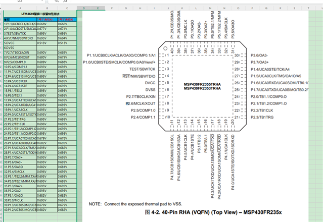
    We have checked the documents in your link. We have made a preliminary inspection on the appearance of the defective material and the characteristics of the pin diode, and we have not found that the material has mechanical stress or electrical stress damage. The following is the table of the protective diode of the pin of the material I tested before. Please refer to it.
    ...

  •  **Attention** This is a public forum

  • Hi huangjian,

    I have sent you an email with all the information. Thanks for providing me with this information, as it is important to review before a return can be processed.

    Best,

    Owen

**Attention** This is a public forum