MSP430FR6047: Significance of Tx bias and Rx bias in USS measurement

Part Number: MSP430FR6047

Tool/software:

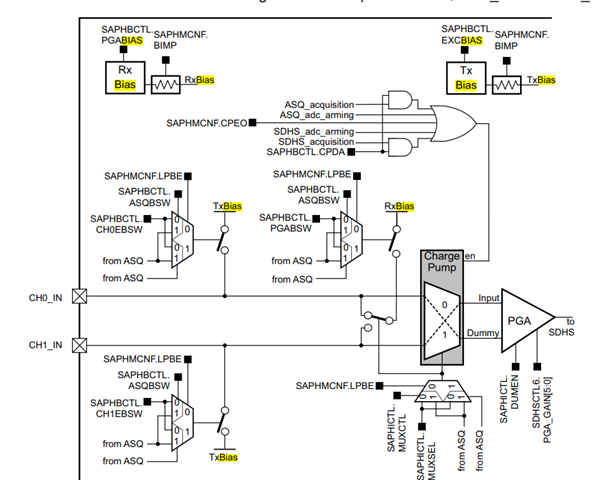
From the diagram, I would like to understand the importance of the Rx Bias and Tx Bias voltages.

  1. Why is biasing needed, especially when the PGA input is limited to a maximum of 800 mVpp?

  2. My understanding is that adding a bias might cause the input to exceed this 800 mVpp limit, depending on signal swing. Should I be concerned about this?

  3. Do I need to carefully consider both Rx and Tx bias settings, or are they internally isolated such that they don’t affect each other directly?

Could you please help clarify how biasing interacts with PGA input range and what precautions should be taken in setting these voltages to ensure the signal remains within allowed limits?

  • Hi,

    1. The RX bias voltage is needed because we do not want negative voltage goes into the MCU. TX bias is used to protect overshoot while excitation. 

    2. You should concern the RX bias voltage plus the receive signal not exceed 800mVpp limit. 

    3. TX and RX bias are internally isolated. They do not affect each other. 

    Best regards,

    Cash Hao

  • So from the datasheet , can i interpret following points.

    1. Since maximum allowed setting for RX bias is 950mV, and maximum allowed swing is 800mV. So the maximum allowed common mode voltage for PGA is 1350mV and 550mV

    2. if i consider a swing of 1000mV it is 1450 to 450mV.

    Is my interpretation correct?. if yes then my input signal +RX bias should honour these ranges so that their is no damage to PGA. In view of the same kindly suggest should i consider 1000mV or 800mV as datasheet suggests for both values

    Secondly suppose my signal +RX bias is well within 1350mV to 550mV, but  above the criteria of 800mv(pk-pk), then in that case what would be the impact on delta tof .

    Consider i have an Input signal of 520mV (0-pk) and i keep RX bias as 750mV, so i pre-assume i am within the common mode specs but 800mV(pk-pk) is not meeting, so what is the long term or short term impact on flow metering. And how can i compensate for this

  • Hi,

    Your interpretation looks correct to me. For PVCC >= 2.5V, you can consider 1000mV. 

    For above the criteria of 800mv(pk-pk), I would say it could impact the tof calculation. 

    An input signal of 520mV (0-pk) could cause signal clipping on the ADC captures. The ADC(SDHS) reference voltage is 755mV. You do not want the ADC input signal exceed this range(0-755mV) to avoid clipping issue. 

    Best regards,

    Cash Hao

  • if ADC reference voltage is +755mV, and if  bias included on AC , then bias voltage itself is equivalent to signa

  • Hi,

    The PGA can be set to negative gain value. Your concern will not be an issue. 

    Best regards,

    Cash Hao 

  • So, I apply bias,voltage level reach to 1350 mV peak and i have to apply negative gain such that the 1350 mV become less than its reference 775 mV?IIs my observation is correct...

  • i want to know that the Gain is applied on (Rx-Bias + Received signal )or only on received signal ?

  • I would say it is applied on both bias and receive signal. 

  • so as per my observation the received signal before gain not more than 1000 mV peak to peak or it means the difference between max peak and min peak not more than 1000mV.And after gain applied the signal must less than 755 mV (0-pk) signal.Is my observation is correct?

  • Yes, after gain applied the signal must less than 755 mV (0-pk) signal. 

  • I have a query regarding the PGA and ADC operation.

    1. Suppose I exceed the PGA differential input voltage specification (±1000 mV), but I reduce the PGA gain such that my ADC input never saturates. In this case, I am violating the PGA input spec but still staying within the ADC input range. Is this an acceptable condition, or will it cause performance issues (linearity, distortion, reliability, etc.)?

    2. Also, I would like to understand why different bias settings are provided in the device. What is the intended use case or trade-off behind selecting different bias modes?

    3. The datasheet mentions a PGA differential input limit of ±1000 mV. Should this be treated as an absolute max, or do we need to keep additional margin (e.g., 800 mV or 900 mV) for long-term robustness? For example, if my system always applies a 930 mV differential input continuously for 10 years, would this still be considered safe and reliable?

    Thank you for your support.

  • Hi,

    1. You will never encounter this case. Because the minimum Gain setting is -6.5dB. With the input voltage as ±1000 mV the output will be ±473 mV which exceeds the 755/2mV = 377.5mV. 

    2. It just needs a bias voltage to let the signal all above 0. It saves a negative voltage rail on the application level. 

    3. It is an absolute max. It is considered safe if you applies a 930mV for 10 years. 

    Best regards,

    Cash Hao

  • From my understanding, the received ADC input signal must be less than 375 mV (0–peak), which corresponds to about 750–800 mV (peak-to-peak). Then why does the datasheet specify that the differential mode limit is 1000 mV (peak-to-peak)?

    Also, in my observation, the ADC reference voltage is 755 mV. Could you please clarify why only half of this value (≈375 mV) is considered as the maximum allowable input to meet the specification, instead of the full 755 mV?

    In our earlier discussion, it was mentioned that the ADC reference is 755 mV.

    • In one place, it was referred to as 0–peak (755 mV).

    • In another place, it was described as peak-to-peak (755 mV).

    This is creating confusion. Could you please clarify:

    1. Whether the 755 mV reference corresponds to full-scale 0–peak or to full-scale peak-to-peak?

    2. Based on this, what should be the maximum allowed differential input signal amplitude to avoid violating the ADC input specification?

  • 755mV corresponds to full-scale 0-peak. 

    For the maximum allowed differential input signal amplitude, let's use 755mV/2 * 10^(6.5/20) = 797.84mV. So the maximum input signal should be ±797.84mV.

  • Above you mentioned, that the effective recommended maximum is about 797.85 mV (depending on reference and PGA settings).

    Previously,you also mentioned that the device could still work properly at around 930 mV differential input. This seems contradictory.

    Point right Can you please clarify:

    • What is the true safe long-term differential input limit for the PGA?

    • Is 930 mV continuous operation over 10 years considered within spec and reliable, or is it already exceeding the recommended safe limit even if the ADC does not saturate?

  • What is the true safe long-term differential input limit for the PGA?

    It is defined in datasheet. ±1000 mV. 

    We are talking about to make the ADC capture data meaningful. We do not want a clipping signal to be captured. So, from this point the requirement is stricter. These are two different aspects. 

  • So i need to make the Recieved signal less than 800mV (pk-pk) for better Results.

  • Yes, it is correct. 

  • 1. You will never encounter this case. Because the minimum Gain setting is -6.5dB. With the input voltage as ±1000 mV the output will be ±473 mV which exceeds the 755/2mV = 377.5mV. 

    In that you mention ±1000 mV which corresponds to 2000 mV peak to peak .As per my observation gain applied on 500 mV so  that it passes the limit of 377.5mV when 1000 mV peak to peak signal .

    please mention that peak to peak voltage limit.Is it 1000 mV peak to peak or 2000 mV peak to peak.

  • I am mention  ±1000 mV as 2000mV peak to peak.

**Attention** This is a public forum