MSP430F5324: Can you review the MSP430F5324 defect report and answer any questions?

Expert 2670 points
Part Number: MSP430F5324
Other Parts Discussed in Thread: MSP-GANG

Tool/software:

Hi All,

Can you review the MSP430F5324 defect report and answer any questions?

[Defect Description]
・The microcomputer was MSP430F5324.
・A market product claim occurred.
As a result of reading the contents written in the defective microcomputer by BSL communication,
the contents of the memory were different from those of the normal product.
The difference is "00 00 is included in some parts and the value is off."

・The cause of the defect is known to be that the correct value was not written in the microcomputer.
・The occurrence rate is being checked.

[Result of checking defective products]
・When trying to verify the defective product by JTAG communication, communication was not possible because the JTAG lock was engaged.
・When trying to verify the defective product by BSL communication, a verify error occurred. (The written content is as described in the above defect content.)
・In the production line, writing errors occasionally occur when writing by JTAG communication.
However, when writing by JTAG again and it is normal, it is used in the product.
In mass production, writing by JTAG communication and if it is normal by verify, JTAG lock is applied.

[Question]
・Is it possible that a problem like this occurs other than writing?
I want to distinguish whether it occurs during microcomputer writing or after it is released to the market
(1) The product writes to Information Memory C and D to memorize settings.
Is it possible that an error occurs during the operation and 00 00 is entered and the value is shifted?
(2) Is it possible that external noise occurs in the product and 00 00 is written and the value is shifted?
(3) Is it possible that 00 00 is written and the value is shifted due to timing shift such as noise during microcomputer writing?

・If there is a movement of "00 00 is entered and the value is shifted partially" like this time in Verify when writing by JTAG communication during mass production,
(1) Can the content of the defective product read this time be detected by Verify of JTAG communication?
(2) Is there a possibility that Verify is recognized as normal by mistake? When can it occur?
From the Verify calculation, is it possible to judge that the Verify value is normal for the written content of this defective product?

・If it is written by JTAG communication at the time of mass production, is it correct that JTAG lock is not applied if Verify abnormality is shown?
Is it possible that JTAG lock is applied even if Verify abnormality is shown?

・Have you heard of such a problem with MSP-GANG? (Other companies, etc.)

・Is there any difference between "Verify with JTAG communication" and "Verify with BSL communication" with MSP-GANG?
(1) Is it possible that this problem is not noticed by Verify with JTAG communication but is noticed by Verify with BSL communication?
(2) Is there a way to perform full verify with JTAG communication of MSP-GANG?
(3) I understand that JTAG communication: PSA comparison, BSL communication: checksum +PSA comparison. Is it correct?

・I am trying to release JTAG lock using BSL communication of MSP-GANG, but I cannot release it.
I understood that it can be released by writing FF FF FF FF FF in memory of @17FC, but once JTAG lock is applied,
Is it possible to restore JTAG communication?
Regarding Memory Options when writing, "All Memory (without BSL sectors), including locked INFO-A"
I pressed Program button, but it was not changed when I read by Read and looked at @17FC.


[Our thoughts]

・I think the tool or power supply in the process of writing to the microcomputer is suspicious, but in that case, can it be detected by Verify? I think so.
・What happens to cause this phenomenon?

① From the content of the defect "00 00 is misplaced," I guessed that the value was likely misplaced when writing to the microcomputer.
However, isn't it possible to detect the abnormality by Verify performed when writing in JTAG communication? If so, isn't it possible that the defective product occurs?

② If Verify abnormality occurs in JTAG communication, it is possible that the erroneous content written in MSP-GANG remains in the microcomputer and causes an error.
However, if Verify abnormality occurs, JTAG lock should not be implemented.
Since JTAG lock was implemented this time, isn't it unlikely that Verify abnormality occurred but was overlooked and incorporated into the product?
⇒ Then, does it mean that Verify passed correctly?
After Verify was normal and JTAG lock was applied, 00 00 writing like this time occurred due to an external factor?
⇒ Or is it possible that JTAG lock is performed even if Verify does not pass correctly?

③ Verify passes correctly at the time of writing, but when Verify is performed later by BSL communication, an error occurs.
Is it possible that Verify becomes normal even if the value is wrong at the time of JTAG writing, and then when Verify is performed again by JTAG communication or BSL communication, a Verify error occurs?

④ If JTAG lock can be released, can this error be detected by Verify in JTAG communication?
During JTAG writing, can this problem occur due to the influence of power supply or noise of the writer?
Is it possible that Verify error does not occur and JTAG lock is applied even if an incorrect value is written?

Best Regards,

Ito

  • Hi Ito,

    Sorry for the late response. I have forwarded the thread to the expert in my team, will get feedback and comment here sooner.

    Thanks for your patience.

    B.R.

    Sal

  • Hi sal,

    Have you received a response from the expert yet?

    My customer is asking about it.

    Best Regards,

    Ito

  • Hi sal,

    Have you received a response from the expert yet?

    My customer is asking about it.

    Best Regards,

    Ito

  • Hi Ito,

    Sorry for late response. I do not receive feedback from the expert.

    So I jump in to respond. See the comments below:

    (1) The product writes to Information Memory C and D to memorize settings.
    Is it possible that an error occurs during the operation and 00 00 is entered and the value is shifted?

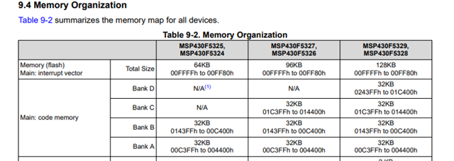
    I am little confused why there will have the write behavior for Memory C and D. As I checked the datasheet description, there only has Memory A and B for MSP430F5324:

    (2) Is it possible that external noise occurs in the product and 00 00 is written and the value is shifted?
    (3) Is it possible that 00 00 is written and the value is shifted due to timing shift such as noise during microcomputer writing?

    I think after it successfully write, the value will be constant unless there has any write behavior in the application code.

    During the write process, there do has possiblity that the value is impact by external noise.

    (1) Can the content of the defective product read this time be detected by Verify of JTAG communication?
    (2) Is there a possibility that Verify is recognized as normal by mistake? When can it occur?
    From the Verify calculation, is it possible to judge that the Verify value is normal for the written content of this defective product?

    ・If it is written by JTAG communication at the time of mass production, is it correct that JTAG lock is not applied if Verify abnormality is shown?
    Is it possible that JTAG lock is applied even if Verify abnormality is shown?

    I don't think so, if the value is read as "00", which is not the expected value, the verify should return error. 

    Let take a discussion with team expert on GANG.

    (3) I understand that JTAG communication: PSA comparison, BSL communication: checksum +PSA comparison. Is it correct?

    JTAG verify works with PSA, while I am not sure BSL verify, maybe just some CRC check. Need double check with GANG expert.

    Let me check if there any possiblity that verify will not notice the firmware error.

    Is it possible to restore JTAG communication?

    I assume you are talking about:

    You can find the way to unlock it: https://www.ti.com/lit/ug/slau320aj/slau320aj.pdf 

    It requries additional operation to unlock it.

    B.R.

    Sal

  • Hi Sal,

    Thank you for your help,

    Could you send the following report to the GANG team?


    [Request]
    ・The cause of the defect is known to be that the correct value was not written to the MSP430F5324.
    Please provide the cause investigation and countermeasures.

    [Issue]
    When reading the contents written to the defective MCU via BSL communication, “00 00” was found, and the values were partially off.

    [Customer Verification Findings]
    ・Reading data via BSL communication from the defective unit revealed the value misalignment.
    ・Attempting to perform Verify via SWB (Fast) communication on the defective unit failed because Secure Device was active.
    (During mass production, writing is performed via SWB (Fast) communication with Secure Device enabled.)
    ・When performing Verify via BSL communication on the defective unit, a Verify error occurred (error details as per the defect description above).
    ・According to the production line, write errors occasionally occur during SWB (Fast) communication writes.
    However, units that passed a subsequent SWB (Fast) communication write are being used in production.


    [Questions]
    1. Is it possible for a defect like this to occur outside of the writing process? (We want to determine if it occurs during microcontroller writing or after the product enters the market).
      Could noise cause 00 00 to be written, shifting the value, outside of the writing process?
     ① Is it possible for external noise to enter the product, causing 00 00 to be written and shifting the value?
     ② Could timing issues like noise during microcontroller programming cause 00 00 to be written, leading to value shifts?

    2. When a Verify error occurs during programming with MSP-GANG, do the values written to the microcontroller remain intact?

    3. Please explain what type of Verify is performed during each communication step when using MSP-GANG for Verify.
    Would the values written to the defective unit sent this time pass Verify?
    Also, is it possible for Verify to pass even with incorrect content due to noise during Verify?
    We believe Verify would not pass with the values written to the defective unit.
    JTAG: PSA comparison
    SWB(Fast): ?
    BSL: Checksum + PSA comparison?

    4. When writing with Secure Device enabled in SWB(Fast),
    After “Software Write” completes, does Verify run? If successful, does Secure Device lock to prevent SWB(Fast) communication?
    Does Secure Device lock even if Verify fails?

    In my view, if Secure Device does not lock even when Verify fails, this issue would not occur.
    I believe Secure Device locked despite the Verify failure.
    Even if an error was missed on the production line, I believe Secure Device would not lock if Verify failed.


    5. Are there methods other than Verilay to detect defective products like this one (where 00 00 is written, causing partial value shifts) during the write process?
    ・ Is it possible to perform “Compare Code File and Flash ROM” after the write operation?
    ・ If the defect frequency decreases, I believe “Performing Verify again after the write operation” could be feasible.


    6. When noise or timing errors cause 00 00 to be written during microcontroller programming,
    Please provide precautions for programming using MSP-GANG's SWB (Fast).

    Example:
    ・Keep the cable length from the MSP-GANG connector to the microcontroller's programming pins under X cm.
    ・Methods to improve noise immunity for the cable and MSP-GANG itself (e.g., reducing SWB speed, shielding copper foil sections).

    Best Regards,

    Ito

  • Hi Ito,

    Can you help share more details of the memeory data issues.

    When reading the contents written to the defective MCU via BSL communication, “00 00” was found, and the values were partially off.

    What memeory address range has this issues?

    What is the expected value? Is the all the failed device has the same failed address, or they are random? And what is failure rate?

    Meanwhile, will the app manually use flash controller to program the specfic address?

    And, may I know how you lock the device - you should load some data into 0x17FC to lock it, correct? 

    B.R.

    Sal

  • Additionally, update some comments regarding as your question post here.

    1. Is it possible for a defect like this to occur outside of the writing process? (We want to determine if it occurs during microcontroller writing or after the product enters the market).

    Yes, out of programming, if there has overspec happens to MCU, such as overvoltage or over current (voltage is more often), then it might make the flash data been tampered with

    2. When a Verify error occurs during programming with MSP-GANG, do the values written to the microcontroller remain intact?

    Yes, verify should only do read and check. Does not impact the firmware itself.

    3. Please explain what type of Verify is performed during each communication step when using MSP-GANG for Verify.

    MSP GANG is not maintain by TI level. I can double check but not for sure to make it clarified well.

    While, I believe if the data is incorrect to your code files, the verify should failed.

    4. When writing with Secure Device enabled in SWB(Fast),
    After “Software Write” completes, does Verify run? If successful, does Secure Device lock to prevent SWB(Fast) communication?
    Does Secure Device lock even if Verify fails?

    What the secure device enabled you means here? Below options?

    5. Are there methods other than Verilay to detect defective products like this one (where 00 00 is written, causing partial value shifts) during the write process?

    The method you have posted here.

    6. When noise or timing errors cause 00 00 to be written during microcontroller programming,
    Please provide precautions for programming using MSP-GANG's SWB (Fast).

    The cable is the most important parts to avoid the noise, recommend to use the included cable with GANG product.

    The longer length should also be good as long as it provide good isolation between signal wires (TDI, TCK, TMS, TDO). Each signal wire is expected to be separated by a DC wire to minimize crosstalk between the signal wires.

    B.R.

    Sal

  • Hi Sal,

    Before answering your question, please allow me to clarify one point.

    Yes, out of programming, if there has overspec happens to MCU, such as overvoltage or over current (voltage is more often), then it might make the flash data been tampered with

    I believe the phenomena described as “a specific value changing to 00”
    and “00 being entered causing the flash contents to shift” are distinct.
    Which of these occurs due to overvoltage or overcurrent?

    Best Regards,

    Ito

  • Hi Ito,

    and “00 being entered causing the flash contents to shift” are distinct.

    This is normamlly due to noise during the firmware loading.

    I believe the phenomena described as “a specific value changing to 00”

    This is more likely due to overspec.

    By the way, please help clarify the details so that I can try to analyze more for this failure. Thanks.

    What memeory address range has this issues?

    What is the expected value? Is the all the failed device has the same failed address, or they are random? And what is failure rate?

    Meanwhile, will the app manually use flash controller to program the specfic address?

    And, may I know how you lock the device - you should load some data into 0x17FC to lock it, correct? 

    B.R.

    Sal

  • Hi Sal,

    Thank you for your help.

    This is normamlly due to noise during the firmware loading.
    This is more likely due to overspec.

    Does “00 being entered causing the flash contents to shift” mean:
    “When writing to the microcontroller using MSP-GANG, if overvoltage or overcurrent occurs, random 00s are inserted and the values shift”?

    Or does it mean:
    “After writing is completed on the product and it is shipped to the market, if overcurrent or overvoltage occurs, 00s are inserted and the values shift”?

    Why does overvoltage or overcurrent cause 00 to be inserted and cause misalignment?
    I want to understand the specific reason or principle behind this.

    What memeory address range has this issues?

    What is the expected value? Is the all the failed device has the same failed address, or they are random? And what is failure rate?

    Meanwhile, will the app manually use flash controller to program the specfic address?

    And, may I know how you lock the device - you should load some data into 0x17FC to lock it, correct? 

    ・I am attaching both the “data experiencing this issue” and “normal data”.
    ・The values will be random.
    ・The failure rate is 2 out of 5000 units.
    ・The address being written via MSP-GANG is All Memory (without BSL sectors).
    ・It is unclear whether data is being loaded into 0x17FC.
    I have included the settings attempted during the unlock process in the documentation.
    (Based on the content, we believe writing is occurring at 0x17FC.)
    The documentation will be sent via private message.
    Although not mentioned in the documentation, we have enabled the Secure Device option within Secure Device Options to apply the lock.
    Attempting to unlock using the methods described in the documentation does not succeed.

    ・Regarding Secure Device, checking the documentation shows that writing is occurring while Secure/Protect is in a state where it cannot be pressed (locked state).

    Best Regards,

    Ito

  • Hi Sal,

    While the JTAG lock is being released, I have an additional question.

    <Question>
    For the MSP432F5324, I configured BSL communication settings using the MSP-GANG GUI.
    Under Memory Options ⇒ Memory Erase/Program…, I set it to
    All memory (without BSL sectors) + including locked INFO-A,
    then pressed the ERASE button, followed by a Read operation.

    I expected that "the BSL area would remain, the JTAG lock-related 0x17FC to 0x17FF would change to FF,
    and all other areas would be erased to FF."

    However, the read result showed that
    the BSL area remained intact, including the JTAG lock-related sectors 0x17FC to 0x17FF,
    while the rest of the memory was erased to FF.
    Consequently, the JTAG lock could not be released.

    Which of the following causes could be responsible?
    - Incorrect settings,
    - MSP-GANG malfunctioning,
    or
    - MSP430F5324 malfunctioning?

    Best Regards,

    Ito

  • Hi Sal,

    Would you mind sharing your opinion?

    Best Regards,

    Ito

  • Hi Sal,

    Would you mind sharing your opinion?

    Best Regards,

    Ito

  • Hi Sal,

    My client is urgently awaiting a response.
    Please provide your opinion.

    Best Regards,

    Ito

  • Hi Ito,

    I am OOO these days.

    I will update some feedback later today.

    B.R.

    Sal

  • Hi Ito,

    “When writing to the microcontroller using MSP-GANG, if overvoltage or overcurrent occurs, random 00s are inserted and the values shift”?

    That is not finalized, we can not guarantee the behavior when the noise or overspec or unstable connection occurs in the programmer.

    Or does it mean:
    “After writing is completed on the product and it is shipped to the market, if overcurrent or overvoltage occurs, 00s are inserted and the values shift”?

    00 might be inserted, but the following values all shifted is hard to occurs.

    I checked the txt files you shared, and I find there has partial flash data shifted, and then it recovered: Only line 982 - line 985 has wrong flash data.

    And what is the function of the code of these specific range?

    BTW, the customer do not verify the function before release it to market?

    Which of the following causes could be responsible?
    - Incorrect settings,
    - MSP-GANG malfunctioning,

    I am not familiar with this kind of approach, and I in following days do not have bandwidth to do some test.

    Have you try it with a EVM board or test board? I can run it in early October.

    B.R.

    Sal

  • Hi Sal,

    Thank you for your help.

    And what is the function of the code of these specific range?

    This is a customer-developed function that sets values for the application.

    BTW, the customer do not verify the function before release it to market?

    The customer has verified and shipped the product without problems.

    Assuming that this problem occurs during writing, I am thinking of investigating overvoltage and overcurrent.
    ・Am I correct in understanding that the supply voltage to the microcomputer is overvoltage?
    ・Is it correct to assume that the voltages of DVCC1 and DVCC2 are MAX4.1V or less (when VSS is GND)?

    Is there a recommended analysis method for overcurrent?

    ・In order to determine whether the MSP-GANG is correctly written,
    are there any signal lines or power supply voltages that should be checked with an oscilloscope?

    ・If overcurrent or overvoltage has been occurring since the product went on the market,
    what are the possible circumstances?

    The power supply to the microcomputer is "24 VDC⇒ 5.8 V by DCDC converter ⇒ 3.3 V by LDO ⇒ MCU," so we think it is unlikely that overvoltage is caused by LDO.

    Best Regards,

    Ito

  • Hi Sal,

    Currently, my customer is performing SBW programming and compare-match verification.
    Additionally, they are considering checking VDD, TDIO, TCK, and GND as part of noise investigation during programming.
    We have not yet received a response regarding the following point, and would appreciate your opinion:
    When using MSP-GANG and MSP430F5324 to program a Secure Device via SBW (Fast),
    if a verify error occurs during programming, will the Secure Device become locked?

    We configured MSP-GANG’s GUI to use BSL communication for the MSP430F5324.
    Under “Memory Options ⇒ Memory Erase/Program…”, we selected
    “All memory (without BSL sectors) + including locked INFO-A”,
    then clicked the ERASE button, followed by a Read operation.

    Our expectation was:
    “The BSL region would remain intact, the JTAG lock-related area (0x17FC–0x17FF) would be set to FF,
    and all other regions would be erased to FF.”
    However, the actual Read result showed that:
    The BSL region, including the JTAG lock-related area (0x17FC–0x17FF), remained intact,
    while all other regions were erased to FF.
    As a result, we were unable to unlock the JTAG.

    Which do you think is the cause:
    an issue with our procedure,
    a malfunction in MSP-GANG,
    or a problem with the MSP430F5324 itself?

    Best Regards,

    Ito

  • Hi Ito,

    Sorry for late response. Just come back from holiday. 

    The customer has verified and shipped the product without problems.

    Assuming that this problem occurs during writing, I am thinking of investigating overvoltage and overcurrent.
    ・Am I correct in understanding that the supply voltage to the microcomputer is overvoltage?
    ・Is it correct to assume that the voltages of DVCC1 and DVCC2 are MAX4.1V or less (when VSS is GND)?

    If it verifed the product function before release to market, what I can suspect is the working environment makes the flash data has been tampered with.

    Altough the shifted flash data is quite weird, for my perspective, it more likely to flash write issues. [If the product has done OTA]

    Is there a recommended analysis method for overcurrent?

    Unfortunately no, this depends on real product enviroment.

    ・If overcurrent or overvoltage has been occurring since the product went on the market,
    what are the possible circumstances?

    Soem suspection from my side, the MCU power has over voltage due to input power surge. The IO input current is larger due to accidental circuit shorten.

    When using MSP-GANG and MSP430F5324 to program a Secure Device via SBW (Fast),
    if a verify error occurs during programming, will the Secure Device become locked?

    Unfortunately we do not have this kind of answers, as this programmer is maintained by Elprotronic.

    I recommend user do test in their side to make it clear.

    B.R.

    Sal

  • Hi Ito,

    We configured MSP-GANG’s GUI to use BSL communication for the MSP430F5324.
    Under “Memory Options ⇒ Memory Erase/Program…”, we selected
    “All memory (without BSL sectors) + including locked INFO-A”,
    then clicked the ERASE button, followed by a Read operation.

    Our expectation was:
    “The BSL region would remain intact, the JTAG lock-related area (0x17FC–0x17FF) would be set to FF,
    and all other regions would be erased to FF.”
    However, the actual Read result showed that:
    The BSL region, including the JTAG lock-related area (0x17FC–0x17FF), remained intact,
    while all other regions were erased to FF.
    As a result, we were unable to unlock the JTAG.

    As for this question, let me double check next week.

    B.R.

    Sal

**Attention** This is a public forum