

hi ti community
I’ve set the capacitive-touch area with a 0.5 mm / 45° hatched ground.
Ground-to-trace clearance is 0.6 mm (taken as t/8), and electrode-to-ground spacing is 2.4 mm (taken as t/2).
The overlay material is 4 mm glass
Layout 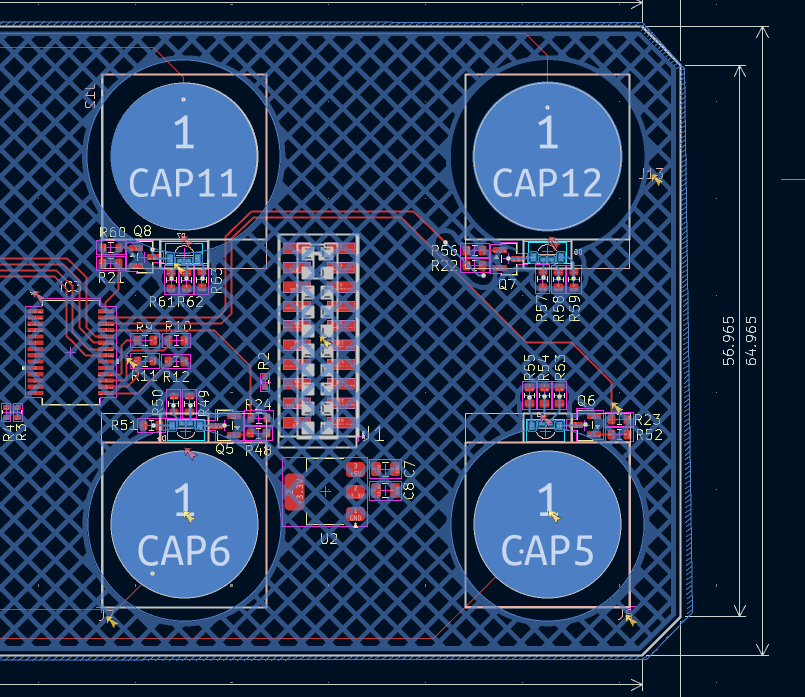 hatch details
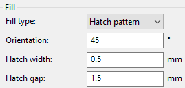
Could you please confirm if these values and this approach are appropriate for capacitive-touch design?

-
Ask a related question
What is a related question?A related question is a question created from another question. When the related question is created, it will be automatically linked to the original question.


