This thread has been locked.

If you have a related question, please click the "Ask a related question" button in the top right corner. The newly created question will be automatically linked to this question.

DRV8363-Q1EVM: Query on DRV8363-Q1EVM compatibility with MSPM0G3519 MCU

Part Number: DRV8363-Q1EVM
Other Parts Discussed in Thread: MSPM0G3519, , LAUNCHXL-F280049C, DRV8363-Q1, DRV8363

Hi,


I am working on a BLDC motor control application using the MSPM0G3519 MCU and have procured the DRV8363-Q1EVM for gate-driver evaluation.

While going through the DRV8363-Q1EVM Quick Start Guide, I noticed the following caution note:
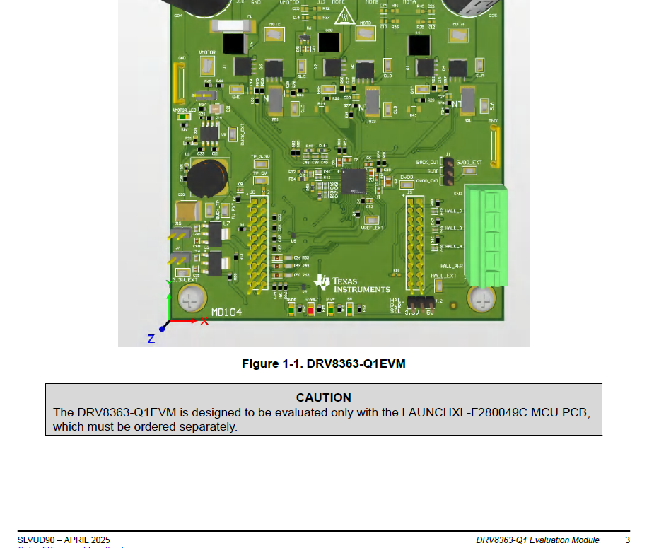
image.png


Currently, I do not have the LAUNCHXL-F280049C board, and I intend to interface the DRV8363-Q1EVM directly with the MSPM0G3519 MCU.

I would like clarity on the following points:

  1. Is the DRV8363-Q1EVM electrically and functionally compatible with MSPM0G3519 for evaluation purposes (SPI + 6-PWM control)?

  2. Does the caution note indicate a hardware limitation, or is it primarily related to official software support and validation from TI?

  3. Are there any specific constraints, risks, or recommended checks when using DRV8363-Q1EVM with a non-C2000 MCU such as MSPM0?

  4. Is there any reference documentation, application note, or recommended validation procedure for bringing up DRV8363-Q1EVM with general-purpose MCUs?

  5. For basic BLDC operation (6-step commutation), is software-based dead-time generation from MSPM0 considered acceptable for evaluation?

My goal is to safely validate the DRV8363-Q1 device and perform low-power BLDC motor control experiments using MSPM0G3519.

I would appreciate your guidance on whether this approach is acceptable and any recommendations you may have.

Thank you for your support.

Best regards,

Sakhan

  • Hey Sakhan,

    The C2000 49C launchpad is the recommended one because of thew compatibility with the EVM Software/GUI, and its what we have tested to work.

    But no, there is nothing preventing you from jumping over the signals from another MCU provided you write its firmware for motor control. 
    We dont have a general purpose MCU bring up guide but as long as the EVM schematic can be used to jump over signals to your MCU's I dont expect it to be much different. 

    For 6 step commutation, you can use MCU deadtime, and or rely on the DRV deadtime (provided your are not using independent mode - no dead time insertion).

    I can pass this thread over to the M0 team to see if they have any guides to bring up with M0 for motor control.

    Best,

    Akshay

  • Hi Sakhan,

    Here is some documentation on motor control with MSPM0:

    Furthermore, our SDK has some motor control examples available:

    Best,

    Owen

  • Hi Owen,

    Can I validate the DRV8363-Q1EVM by generating PWM and basic GPIO signals (like nSLEEP ..etc) without using SPI, and will this be sufficient to verify the driver’s functionality?

    Regards,

    SaKhan

  • Hi SaKhan,

    Based on the DRV6383-Q1 datasheet, SPI is used for setting device configurations, operating parameters, and reading out diagnostic information.

    If you need further support on this, I can loop in the motor drive team on this thread.

    Best,

    Owen

  • Hi Owen,

    I’d appreciate it if you could add the motor drive team to this thread.

    Regards,

    Sakhan.

  • It would be great if I could get an application note for the DRV8363S SPI implementation for each mode, including the register configuration.

  • Hi Sakhan,

    I have just added the motor drive team to the thread.

    Best,

    Owen

  • Hey Sakhan,

    The basic device bring up and functionality can be done without SPI, by using the default register configurations. 

    We dont have an application not for the SPI configs but the definitions and the default configurations are shown in the datasheet SPI table.

    Best,
    Akshay

  • Hi Akshay,

    Thank you for the clarification.

    Could you please explain the basic device bring up and functionality in more detail? It would be helpful if you could outline the steps involved, including how the device initializes and operates using the default register configurations without SPI.

    How to reset the DRV8363 to bring all the register to default values.

    Regards,

    SaKhan

  • Hi Akshay,

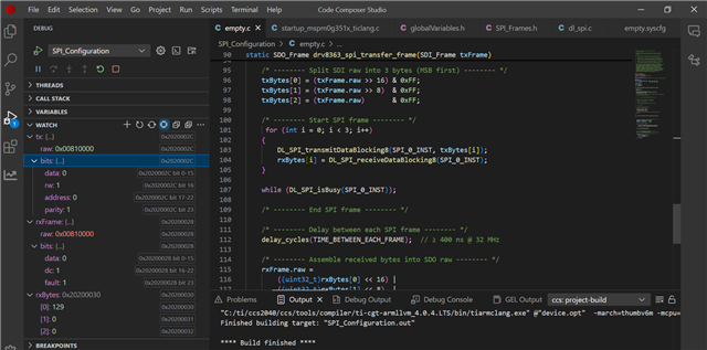
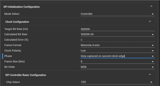
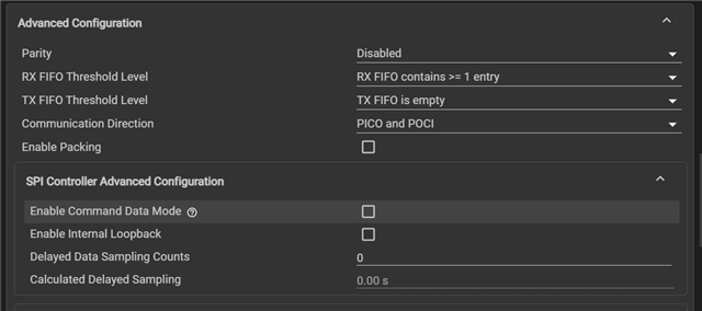
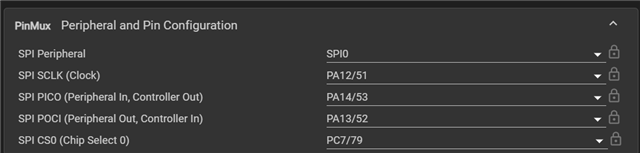
    I have configured the MSPM0 SPI controller to send the DRV8363 SPI frames.

    IC_STAT1 Register (Offset = 0h) [Reset = 8080h]

    Now Address of IC_STAT1 Register is 0x00 (Offset = 0h).

    RW is 1

    Data is 0x0000 

    Parity is 1

    1. The frame formed as per the DRV SDI Frame format (24 bits). Verified the SPI Tx and Rx by Enabling the Internal Loop Mode before connecting to DRV8363.

    2. Code Section

    #include "SPI_Frames.h"
    #include "globalVariables.h"
    #include "ti_msp_dl_config.h"
    #include <ti/driverlib/m0p/dl_interrupt.h>
    
    #define SPI_PACKET_SIZE 8
    #define TIME_BETWEEN_EACH_FRAME 13 // 400ns is 13, 1us is 32 (as per DRV datasheet)
    
    SDI_Frame tx;
    SDO_Frame rxFrame;
    uint8_t gTxPacket[SPI_PACKET_SIZE] = {0x11, 0x22, 0x33, 0x44,
                                          0x55, 0x66, 0x77, 0x88};
    uint32_t sendBytes;
    uint8_t i;
    uint8_t sdi[3];
    uint8_t txBytes[3];
    uint8_t rxBytes[3];
    
    //func proto
    static SDO_Frame drv8363_spi_transfer_frame(SDI_Frame txFrame);
    
    int main(void) {
      SYSCFG_DL_init();
    
      //nSLEEP to "HIGH" (Enable the DRV)
      DL_GPIO_setPins(GPIO_GRP_0_PORT, GPIO_GRP_0_PIN_B12_PIN);
      drv8363_ReadFrame(&tx, 0x00);
      
    
        drv8363_spi_transfer_frame(tx);
    
        drv8363_ReadFrame(&tx, 0x00);
        
        drv8363_spi_transfer_frame(tx);
    
      while (1) {
      }
    }
    
    static SDO_Frame drv8363_spi_transfer_frame(SDI_Frame txFrame)
    {


        /* -------- Split SDI raw into 3 bytes (MSB first) -------- */
        txBytes[0] = (txFrame.raw >> 16) & 0xFF;
        txBytes[1] = (txFrame.raw >> 8)  & 0xFF;
        txBytes[2] = (txFrame.raw)       & 0xFF;
    
        /* -------- Start SPI frame -------- */
         for (int i = 0; i < 3; i++)
        {
            DL_SPI_transmitDataBlocking8(SPI_0_INST, txBytes[i]);
            rxBytes[i] = DL_SPI_receiveDataBlocking8(SPI_0_INST);
        }
    
        while (DL_SPI_isBusy(SPI_0_INST));
    
        /* -------- End SPI frame -------- */
    
    
        /* -------- Assemble received bytes into SDO raw -------- */
        rxFrame.raw =
            ((uint32_t)rxBytes[0] << 16) |
            ((uint32_t)rxBytes[1] << 8)  |
            ((uint32_t)rxBytes[2]);
    
        return rxFrame;
    }


    3. Verified the PICO pin data using the Picoscope. There are 48 rising edge (Each frame = 24 clock rising edge) 

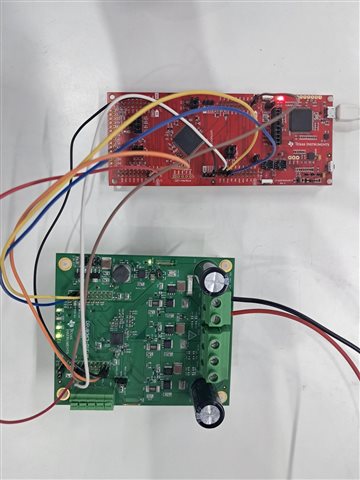
    4. Now, connected the DRV8363 with proper pin mapping. [SPI CLK to DRV SCLK, SPI CS to nSCS, SPI PICO to SDI, SPI POCI to SDO]

    Also, the nSLEEP made HIGH to clear Fault Pin after power up. Refer the below MSPM0 and DRV setup,

    When I send the read frame [0x810000] to DRV there is no response (nothing recieved in Rx register) why? Even I achieved delay between each frame sent to MSPM0 to DRV (Refer the Picoscope data).

    I am not getting the data from the DRV even after sending required frames? 

    Kindly help me on this.

    Regards,

    SaKhan

  • Hey Sakhan,

    Is the green chipselect? it should go high once per word (24 bits).

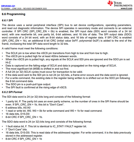
    Have you checked out the DS section 6.6 Programming 6.6.1 SPI?

    Best,

    Akshay

  • Akshay,

    1. I have added my device setup, MSPM0 configuration and frame validation using Picoscope. Please have a look above my response for all details.

    2. From MSPM0, I have validated the Tx and Rx code by send data from PICO and received in POCI using Internal Loopback. As expected the Tx frame recieved in Rx buffer.

    3. When I connect the DRV, I am not getting response for the Tx frame send by MSPM0. Please check all post above and tell me where I am doing wrong like Pin mapping or wrong SPI mode setup or anything. Please guide me to solve this.

    4. I have asked you about the basic functionality (BLDC or BDC) test to prove the DRV is working as expected. Tell me the way to check the functionality with SPI.

    Regards,

    SaKhan

  • The photo doesn't zoom very well, but I think I don't see anything connected to the PA14 (PICO) pin on J1.2. 

    Alternatively: maybe the wire is connected to J1.2, in which case I don't see a 3V3 connection.

  • Hey Sakhan,

    Here is the SPI format for the DRV8363.


    Default: NO CRC, 24 bits.


    0 000000 0 00000000 00000000


    Parity bit – 1 or 0 depending on other 23 bits of the data + r/w + addr. Want the TOTAL number of 1s to be EVEN.


    6 bit Address – 6 bits of the address you are reading/writing to.


    Read/Write bit – 0 for write, 1 for read command.


    16 bit data – Data to write. Can leave 0 for Spi read.


    Our EVM code for the 8363 read/write functions:

     ........................................................................

    Uint32 spi_read(Uint16 addr)

    {

        Uint16 commandword = 0;

        Uint32 p_addr = addr;

        Uint16 p_data = 0;

        Uint16 byte0_r;

        Uint16 byte1_r;

        Uint16 byte2_r;

        Uint16 new_addr;

        Uint16 temp;

        Uint16 temp2;

        Uint16 temp3;

        Uint32 readback;


        //creating full word to calculate parity bit

        Uint32 calc = ((p_addr << 17) & 0x7E0000) | (0x10000) | (p_data & 0xFFFF);

        Uint16 parity = 0;

        while(calc)

        {

           parity ^= (calc & 1);

           calc >>= 1;

        }

        //0 000000 0 0000000000000000, (8363 spi: 1b parity -> 6b addr -> 1b R/W -> 16b data)

        new_addr = addr << 1;

        byte0_r = (parity << 7) | (new_addr & 0x7E) | (0x01);

        byte1_r = 0x00;

        byte2_r = 0x00;


        commandword = (byte0_r << 8);

        SpiaRegs.SPITXBUF=commandword; //transmit top 8 bits

        temp = SpiaRegs.SPIRXBUF;


        //

        commandword = (byte1_r << 8);

        SpiaRegs.SPITXBUF=commandword; //transmit mid 8 bits

        temp = SpiaRegs.SPIRXBUF;


        commandword = (byte2_r << 8);

        SpiaRegs.SPITXBUF=commandword; //transmit lower 8 bits

        temp = SpiaRegs.SPIRXBUF;


        while(SpiaRegs.SPIFFRX.bit.RXFFST != 3); //wait for 3 words to receive in FIFO


        temp = SpiaRegs.SPIRXBUF;

        temp2 = SpiaRegs.SPIRXBUF;

        temp3 = SpiaRegs.SPIRXBUF;


        readback = (temp << 16)|(temp2 << 8)|(temp3);


        return readback;

    }


    Uint32 spi_write(Uint16 addr, Uint16 data)

    {

        Uint16 commandword = 0;

        Uint16 byte0_j;

        Uint16 byte1_j;

        Uint16 byte2_j;

        Uint32 temp;

        Uint32 temp2;

        Uint32 temp3;

        Uint16 new_addr;

        Uint32 p_addr = addr;

        Uint32 readback;

        // R/W = 0b for write command


        //creating full word to calculate parity bit

        Uint32 calc = ((p_addr << 17) & 0x7E0000) | (data & 0xFFFF);

        Uint16 parity = 0;

        while(calc)

        {

           parity ^= (calc & 0x01);

           calc >>= 1;

        }


        new_addr = addr << 1;

        byte0_j = (parity << 7) | (new_addr & 0x7E);

        byte1_j = (data & 0xFF00) >> 8;

        byte2_j = (data & 0x00FF);


        //transmit top 8 bits, shift lef by 8 because TX buffer wants left justified data

        commandword = (byte0_j << 8);

        SpiaRegs.SPITXBUF = commandword;

        temp = SpiaRegs.SPIRXBUF;


        //transmit mid 8 bits, shift by 8 because TX buffer wants left justified data

        commandword = (byte1_j << 8);

        SpiaRegs.SPITXBUF = commandword;

        temp2 = SpiaRegs.SPIRXBUF;


        //transmit lower 8 bits, shift by 8 because TX buffer wants left justified data

        commandword = (byte2_j << 8);

        SpiaRegs.SPITXBUF = commandword;


        while(SpiaRegs.SPIFFRX.bit.RXFFST != 3); //wait for all 3 words to be recieved in FIFO


        temp3 = SpiaRegs.SPIRXBUF;


        readback = (temp << 16) | (temp2 << 8) | (temp3);

        return readback;

    }

     ..................................
    The best way to confirm if the SPI works correclty is to adjust the Idrive registers. By switching between higher and lower IDrive setting sand measuring the SHx-Gnd waveform you can see if the faster gate current is affecting the slew rate. T(rise/fall) = Qgd / I(source/sink)


    Dont recommend using the fastest Idrive setting unless MOSFET QGD is very large.

    Best,

    Akshay

**Attention** This is a public forum