This thread has been locked.

If you have a related question, please click the "Ask a related question" button in the top right corner. The newly created question will be automatically linked to this question.

SPI woes : Waveform meaning ??

Other Parts Discussed in Thread: MSP430F2619

Hi,

For quite some time i have been trying to communicate (write the required hex word) to the AD9834, a Sig-Generator IC.

But i have been unsuccessful.

During subsequent experimentation with the code, i decided to capture the waveforms of the CLK, SIMO and SOMI pins.

The datasheet of the AD9834 states that "After FSYNC (SOMI) goes low, serial data is shifted into the input shift register of the device on the falling edges of SCLK for 16 clock pulses. FSYNC (SOMI) can be taken high after the 16th falling edge of SCLK"

Now i captured all the three signals during program execution, and this is how they look.


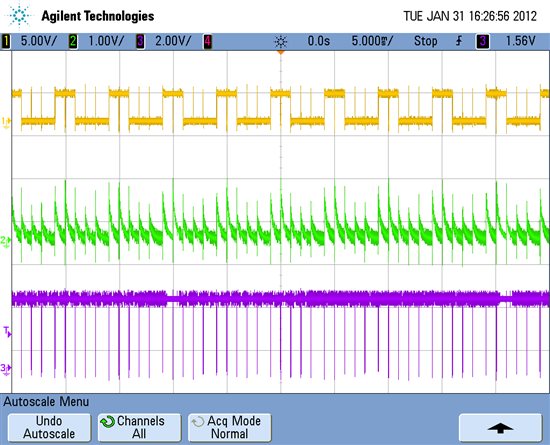
Top/ 1 / yellow = SIMO pin

Middle / 2 / Green = SOMI pin

Bottom / 3 / purple = CLK pin

The clk waveform looks weird to me.

I have the following doubts?

1) Does the CLK waveform look satisfactory?

2) Are my initializations correct?

3) What are the possible reasons because of which my code fails to work?

I would be eternally grateful, if someone could help me out.


PS : (I, II, III, IV and V are the 16bits of data (words) i am entering)

The Code:

#include  <msp430x26x.h>

void main (void)

{
volatile unsigned int i;
WDTCTL = WDTPW+WDTHOLD;                   // Stop watchdog timer
BCSCTL1 = CALBC1_1MHZ;                    // Set DCO
DCOCTL = CALDCO_1MHZ;
for(i=2100;i>0;i--);                      // Wait for DCO to stabilize.

// initialization of port pins

P1DIR = 0xC0;
P1OUT = 0xC0;
P2DIR = 0x00;
P2OUT = 0x00;
P3SEL = 0x0E;
P3DIR = 0x0E;
P3OUT = 0x0E;
P5SEL = 0X0E;
P5DIR = 0x0E;
P5OUT = 0x0E;

// initialization concerned with UCBO

UCB0CTL0 |= UCMST+UCSYNC+UCCKPL+UCMSB;    //3-pin, 8-bit SPI master
UCB0CTL1 |= UCSSEL_2;                     // SMCLK
UCB0BR0 = 0x02;                           // /2
UCB0BR1 = 0;                              //
UCB0CTL1 &= ~UCSWRST;                     // **Initialize USCI state machine**
IE2 |= UCB0RXIE;                          // Enable USCI_A0 RX interrupt

// initialization concerned with UCB1

UCB1CTL0 |= UCMST+UCSYNC+UCCKPL+UCMSB;    //3-pin, 8-bit SPI master
UCB1CTL1 |= UCSSEL_2;                     // SMCLK
UCB1BR0 = 0x02;                           // /2
UCB1BR1 = 0;                              //
UCB1CTL1 &= ~UCSWRST;                     // **Initialize USCI state machine**
UC1IE |= UCB1RXIE;                          // Enable USCI_A0 RX interrupt

// Initialize buffers

UCB0TXBUF = 0x00;
UCB1TXBUF = 0x00;

_BIS_SR(LPM0_bits+GIE);
}

#pragma vector=USCIAB0RX_VECTOR
__interrupt void USCIA0RX_ISR (void)
{
  volatile unsigned int i;

  while (!(IFG2 & UCB0TXIFG));              // USCI_B0 TX buffer ready?
 
  while (!(UC1IFG & UCB1TXIFG));              // USCI_B1 TX buffer ready?
 
  P1OUT &= ~0xC0;
 
  // I start
  P3OUT = 0x0A;
  P5OUT = 0x0A;
  UCB0TXBUF = 0X21;
  UCB0TXBUF = 0X00;
  UCB1TXBUF = 0X21;
  UCB1TXBUF = 0X00;
 
  for(i=50;i>0;i--);
 
  P3OUT = 0x0E;
  P5OUT = 0x0E;
  for(i=50;i>0;i--);
  // I ends
 
  // II start
 
  P3OUT = 0x0A;
  P5OUT = 0x0A;
  UCB0TXBUF = 0X50;
  UCB0TXBUF = 0XC7;
  UCB1TXBUF = 0X50;
  UCB1TXBUF = 0XC7;
 
  for(i=50;i>0;i--);
 
  P3OUT = 0x0E;
  P5OUT = 0x0E;
  for(i=50;i>0;i--);
 
  // II ends
 
  // III start
 
  P3OUT = 0x0A;
  P5OUT = 0x0A;
  UCB0TXBUF = 0X40;
  UCB0TXBUF = 0X00;
  UCB1TXBUF = 0X40;
  UCB1TXBUF = 0X00;
 
  for(i=50;i>0;i--);
 
  P3OUT = 0x0E;
  P5OUT = 0x0E;
  for(i=50;i>0;i--);
  // III ends
 
  // IV start
 
  P3OUT = 0x0A;
  P5OUT = 0x0A;
  UCB0TXBUF = 0XC0;
  UCB0TXBUF = 0X00;
  UCB1TXBUF = 0XC0;
  UCB1TXBUF = 0X00;
 
  for(i=50;i>0;i--);
 
  P3OUT = 0x0E;
  P5OUT = 0x0E;
  for(i=50;i>0;i--);
  // IV ends
 
  // V starts
 
  P3OUT = 0x0A;
  P5OUT = 0x0A;
  UCB0TXBUF = 0X20;
  UCB0TXBUF = 0X00;
  UCB1TXBUF = 0X20;
  UCB1TXBUF = 0X00;
 
  for(i=50;i>0;i--);
 
  P3OUT = 0x0E;
  P5OUT = 0x0E;
  for(i=50;i>0;i--);
 
  // V ends
 
  for(i=30;i>0;i--);
 
  }


  •  Hi Janmay, you posted twice the same, this is again the same you get troubled in the old thread, please post again exact MSP part number and where you connected spi signal.

     On track picture of your scope I see there where some spikes superimposed over all track, clk is high state and no data exchanged with device. Clock is generated just when transaction start so check where spikes come from and correct grounding or simply add some rule to trigger to don't fire on short spikes.

     Your program still has issue but I don't remember where spi was and what I suggested to do, first check PxSEL bit where spi is connected to.

     When port selection is ok correct delay loop, don't delay some time BUTwait complection flag or wait IRQ.

     Regards

     Roberto

  • janmay b c said:

    Hi,


     Also on scope image please sample with more detail and post again a two division of this image enlarged to see what happen on division 2 to 4 numbering  with zero at border.

     Are you using a switching PSU near your board?

     Regards

  • janmay b c said:
      P3OUT = 0x0A;
      P5OUT = 0x0A;
      UCB0TXBUF = 0X50;
      UCB0TXBUF = 0XC7;
      UCB1TXBUF = 0X50;
      UCB1TXBUF = 0XC7;
     
      for(i=50;i>0;i--);
     
      P3OUT = 0x0E;
      P5OUT = 0x0E;
      for(i=50;i>0;i--);

     Hi what this means to?

     PxSEL for both are set to 0x0e so both port pin are assigned to alternate function and out port just drive pull Up/Down, I can imagine spikes we see can come from there.

    janmay b c said:
    BCSCTL1 = CALBC1_1MHZ;                    // Set DCO
    DCOCTL = CALDCO_1MHZ;
    for(i=2100;i>0;i--);                      // Wait for DCO to stabilize.

    Dco is stable on next instruction fetch, no need to delay, every case when you stop it resume on Irq @full speed after 1uS

    janmay b c said:
    // II start
     
      P3OUT = 0x0A;
      P5OUT = 0x0A;
      UCB0TXBUF = 0X50;
      UCB0TXBUF = 0XC7;
      UCB1TXBUF = 0X50;
      UCB1TXBUF = 0XC7;
     
      for(i=50;i>0;i--);


    Again don't assume time is enough, wait for send complection then fill buffer fetching from an array or write some base function sending a byte of data and send them sequentially.

     SPI programming is a complex task, just start sending one byte and be sure it work good, then add two bytes and check again with a known sequence.

     To check your DDS start do it with bit banging and see if it work right. If you don't need do some fast modulation task then all is fine also if slow.

     Do you have some data analysis on scope?

     Regards

     Roberto

  • Hi Roberto,

    Thanks for the quick reply.

    Roberto Romano said:
    you posted twice the same

    sorry about that.

    Roberto Romano said:
    please post again exact MSP part number and where you connected spi signal.

    MSP430F2619, SPI connected to 

    UCBOSIMO = P3.1

    UCBOSOMI = P3.2

    UCBOCLK = P3.3

    UCB1SIMO = P5.1

    UCB1SOMI = P5.2

    UCB1CLK = P5.3. Hope this helps.

    best wishes

    janmay

  • Roberto Romano said:

      P3OUT = 0x0A;
      P5OUT = 0x0A;
      UCB0TXBUF = 0X50;
      UCB0TXBUF = 0XC7;
      UCB1TXBUF = 0X50;
      UCB1TXBUF = 0XC7;
     
      for(i=50;i>0;i--);
     
      P3OUT = 0x0E;
      P5OUT = 0x0E;
      for(i=50;i>0;i--);

     Hi what this means to?

    [/quote]

    I need to make SOMI pin low before sending data. That's why i am making bit Px.2 low in each case.

    Roberto Romano said:
    Again don't assume time is enough, wait for send complection

    How will i know how much time i should wait/ give delay?

    Roberto Romano said:
     Do you have some data analysis on scope?

    I dont know what data analysis feature does, so i guess my scope does not have it.

  • Roberto Romano said:
    PxSEL for both are set to 0x0e so both port pin are assigned to alternate function and out port just drive pull Up/Down, I can imagine spikes we see can come from there.

    How i have understood programming :

    PxSEL = 0x0E // bits Px.1/2/3 are selected/ made high

    PxDIR = 0x0E // bits Px.1/2/3 are switched to output direction

    PxOUT = 0x0E  // bits Px.1/2/3 are switched to output direction (part of intialization) 

    NOW, if i want to make bit 2 low before sending data.

    I write PxOUT = 0x0A // bit 2 is low

    If my understanding is wrong, please let me know before its too late. Thanks

  • janmay b c said:

    MSP430F2619, SPI connected to 

    UCBOSIMO = P3.1

    UCBOSOMI = P3.2

    UCBOCLK = P3.3

    UCB1SIMO = P5.1

    UCB1SOMI = P5.2

    UCB1CLK = P5.3

     Hi Janmay, again there where some confusion we need narrow down to single wire:

     Yellow marked bit connect to P3.x and belong to channel B instance 0

     Green marked bit connect to P5.x and belong to channel B instance 1

    Which channel is connected to DDS chip? Why are you using both instance of channel B?

     I hope you know about how dds work:

    http://www.analog.com/library/analogDialogue/archives/38-08/dds.pdf

    http://kb8ojh.net/

    http://www.pudn.com/downloads181/sourcecode/embed/detail841842.html   A complete MSP430 software defined radio project using AD9851.

    http://www.analog.com/static/imported-files/data_sheets/AD9834.pdf

    http://www.ti.com/lit/ug/slau144i/slau144i.pdf

     From AD9834 and chapter 16 of user guide slau144 you can see how to program SPI:

      Data sampled on falling edge, clock start high and MSB transmitted first so, Fsynk go low before to transmit MSB and return High after transmit of LSB :

     Master mode  UCMST =1

    start high & falling edge  select CKPL = 1 CKPH =1

      MSB first  UCMSB =1

     SPI 3 pin mode and Generate SCE for FSYNK (external done) on an I/O pin For example I assume P3.4

    P3 Related  P5 Related   Just change channel number

    --------------------------------------------------------------   Code examples start after this line -----------------------

    /* Embed this comment in your code

       MSP PIN            ->   AD9834

    P3.1 UCBOSIMO -> SDATA

    P3.2 UCBOSOMI -> NC

    P3.3 UCBOCLK  -> SCLK

    P3.4 XXXXXXX  ->  FSYNC

    */

    ===== init of SPI

    P3OUT |= BIT4; // Start Fsynk high

    //  Leave this register first, init must start with reset bit set

    UCB0CTL1 = UCSSEL2 | UCSWRST; // SMCLK clock master reset

    UCB0CTL0 = UCCKPH | UCCKPL | UCMSB | UCMST | UCMODE0 | UCSYNC; // SPI 3 wire clock high sample on falling edge MSB first 8 bit

    UCB0BR0 = 1; // Divisor clock => selected clock

    UCB0BR1 = 0;

    UCB0CTL1 &= ~UCSWRST; // Release reset

    ===== SPI ready

    // ---------------   Send word to AD9834  ------------------

     void AD9834sendwrd(const unsigned int x)

    {

     // if AD9834 is the only SPI connected remove the two line

       while(UCB0STAT&UCBUSY)

          ; // Check ( if noother spi used then wait till SPI finished transmitting ??? Must enter here on IDLE

      P3OUT &= ~BIT4; //  Start with Fsynk LOW

      UCB0TXBUF = (x>>8)&0xff; // transmit High byte

      while (!(IFG2 & UCB0TXIFG))  // (!(UC1IFG&UCB1TXIFG))  // warning channel 0/1 bit are on different register!!

        ; // Wait tx buffer is empty (High bit)

      UCB0TXBUF = x&0xff; // transmit Low byte

       while(UCB0STAT&UCBUSY)

          ; // wait till SPI finished transmitting

      P3OUT |= BIT4; // Finish with Fsynk high

    }

    //*********   on Main   **********

    /* From analog devices AN-1070

    Table 1.
    Hexadecimal Binary
    0x2100 0010 0001 0000 0000
    0x50C7 0101 0000 1100 0111
    0x4000 0100 0000 0000 0000
    0xC000 1100 0000 0000 0000
    0x2000 0010 0000 0000 0000

    */

    AD9834sendwrd (0x2100);  // Control register sine mode

    AD9834sendwrd(0x50c7);  // Frequency register LSB

    AD9834sendwrd(0x4000); // Frequency register MSB

    AD9834sendwrd(0xc000); // Phase Register 0

    AD9834sendwrd(0x2000); // Exit Reset

    ---------------------------------------------    Code stub example end  -----------------------------------------------

     From here you can try program other register and enjoy, please tell me if this can solve your troubles.

     Regards

     Roberto

  • janmay b c said:

    PxDIR = 0x0E // bits Px.1/2/3 are switched to output direction

    PxOUT = 0x0E  // bits Px.1/2/3 are switched to output direction (part of intialization) 

    PxDIR set direction but PxSEL can or cannot superimpose so you can have input in SIMO or SOMI regardless of PxDIR, good practice is to set correct direction too.

     PxOUT, see data sheet pin diagram if not disabled drive the resistor, all depend on PxREN to have pullup/down (PxBIT 1/0) or open.

     Regards

     Roberto

  • Thanks a lot for the exhaustive reply sir, i am very much grateful to you for helping me. Thanks once again. :-)

    Roberto Romano said:
    Which channel is connected to DDS chip? Why are you using both instance of channel B?

    This is because i am using two DDS chips. one connected to UCB0 and the other to the UCB1 channel. My project requires me to generate a sine and a cosine wave simultaneously, hence the two DDS chips.

    I will try once again with the code given by you, and let you know as soon as possible.

    best wishes

    janmay

  • Roberto Romano said:
    P3.4 XXXXXXX  ->  FSYNC

    Unfortunately i will not be able to use P3.4 pin of MSP430F2619 as the FSYNC pin, this is because my PCB has the P3. 1/ 2 / 3 pins already soldered to the 13, 14, 15 (SDATA, SCLK, FSYNC ) pins of the AD9834 chip.

    So, i will have to use the P3.2 (UCBOSOMI) pin as the FSYNC pin.

    best wishes

    janmay

  • janmay b c said:

    So, i will have to use the P3.2 (UCBOSOMI) pin as the FSYNC pin.

     Ok to be sure change BIT4 to BIT2 and leave PxSEL bit 2 at 0  to assign bit to I/O port and not to SPI.

     To generate sine cosine you don't need two spi but just one and two separated FSYNK on same port to leave both channel in sinc releasing reset at same rising edge, best way to do this is to do load different value in the phase register.

     Try if two SPI has acceptable JItter otherwise try open one port of SPI pin and wire the two unit together.

     Regards

  • Dear Sir,

    Thanks a lot for your advice. Also i am grateful to you for sharing the code with me. Here is my final code. Unfortunately i am still unable to get a sine wave output from the AD9834.

    /*
    Code for programming one frequency of the AD9834.

    */
    /* From analog devices AN-1070

    Table 1.
    Hexadecimal Binary
    0x2100 0010 0001 0000 0000
    0x50C7 0101 0000 1100 0111
    0x4000 0100 0000 0000 0000
    0xC000 1100 0000 0000 0000
    0x2000 0010 0000 0000 0000

    */
    #include <msp430x26x.h>


    /* MSP430F2619 PINS --------------> AD9834_1

    P3.1 UCBOSIMO -> SDATA

    P3.2 UCBOSOMI -> FSYNC

    P3.3 UCBOCLK -> SCLK

    P1.6 /OE1 -> Active low enable

    */
    void AD9834sendwrd(const unsigned int X);
    void main (void)

    {
    volatile unsigned int i;
    WDTCTL = WDTPW+WDTHOLD; // Stop watchdog timer
    BCSCTL1 = CALBC1_1MHZ; // Set DCO
    DCOCTL = CALDCO_1MHZ;

    P3SEL |= 0x0A; // P3.3,1 option select 0000 1010
    P1OUT |= BIT6; // Buffer Enable high or 1. There is a active low enabled buffer in
                               between DDS and MSP430

    for(i=50;i>0;i--); // Delay

    P1OUT &= ~BIT6; // Buffer Enable Low or 0


    P3OUT |= BIT2; // Start Fsync high

    UCB0CTL1 = UCSSEL_2 | UCSWRST; // SMCLK clock master reset

    UCB0CTL0 = UCCKPH | UCCKPL | UCMSB | UCMST | UCMODE0 | UCSYNC; // SPI 3 wire clock high,sample on falling edge MSB first 8 bit

    UCB0BR0 = 1; // Divisor clock => selected clock

    UCB0BR1 = 0;

    UCB0CTL1 &= ~UCSWRST; // Release reset

    IE2 |= UCB0RXIE; // Enable USCI_A0 RX interrupt

    AD9834sendwrd(0x2100); // Control register sine mode

    AD9834sendwrd(0x50c7); // Frequency register LSB

    AD9834sendwrd(0x4000); // Frequency register MSB

    AD9834sendwrd(0xc000); // Phase Register 0

    AD9834sendwrd(0x2000); // Exit Reset

    // _BIS_SR(LPM0_bits + GIE); // CPU off, enable interrupts
    }

    //#pragma vector=USCIAB0RX_VECTOR
    //__interrupt void USCIA0RX_ISR (void)
    //{

    void AD9834sendwrd(const unsigned int X)

    {


    while(UCB0STAT&UCBUSY)

    ; // Check ( if noother spi used then wait till SPI finished transmitting ??? Must enter here on IDLE

    P3OUT &= ~BIT2; // Start with Fsynk LOW

    UCB0TXBUF = (X>>8)&0xff; // transmit High byte

    while (!(IFG2 & UCB0TXIFG)); // Wait TX buffer is empty (High bit)

    UCB0TXBUF = X&0xff; // transmit Low byte

    while(UCB0STAT&UCBUSY); // wait till SPI finished transmitting

    P3OUT |= BIT2; // Finish with Fsynk high

    }
    
    
    My schematics: The 74HC244 is the buffer.

    The MSP430 pins:

    Thanks in advance.
  •  Hi Janmay, I send you a bill ;)

     Port P1 P2 P3 are not initialized, I assumed your programming skill and MSP knowledge was more than newbie, still RESET must be asserted then released and also check sleep pin remain at low level, every case connect an 1K resistor from pin12 to ground, otherwise AS9834 can enter sleep mode.

     When checked pin 12 is low try this revised code..

    0131.ad9834.zip

     Regards

     Roberto

  • Dear Sir,

    IT WORKS !!.

    You sir, are truly awesome. Thanks a gazillion. You have helped and taught me a lot during this past week. I was stuck in the same situation for the last month. Its people like you who make this world a better place.

    I am very grateful for your help sir. And yes, my programming skills are miniscule and i am in the process of honing it. I very much appreciate the time that you have taken to go through my schematics and help me with the code. Thanks a lot sir.

    Here's my final code (working !!) which i am using right now to program both my DDS chips. I have not changed the phase register values. I have to change it, to get a cosine wave on the second DDS IC.

    /********************************************************
    ** Code for programming one frequency(sine & cosine) of the AD9834. **
    *********************************************************/


    #include <msp430x26x.h>


    // Function prototypes
    void AD9834sendwrd(const unsigned int X);

    void adportinit(void);

    void AD9834sword(const unsigned int Y);

    void adportinitcos(void);

    void main (void)
    {
    //volatile int i;
    WDTCTL = WDTPW+WDTHOLD; // Stop watchdog timer
    BCSCTL1 = CALBC1_1MHZ; // Set DCO
    DCOCTL = CALDCO_1MHZ;

    adportinit(); // init ad9834 #1 port

    adportinitcos(); // init ad9834 cosine port
    // Start programming
    /* From analog devices AN-1070 programming word sequences
    Table 1.
    Hexadecimal Binary
    0x2100 0010 0001 0000 0000
    0x50C7 0101 0000 1100 0111
    0x4000 0100 0000 0000 0000
    0xC000 1100 0000 0000 0000
    0x2000 0010 0000 0000 0000
    */

    AD9834sendwrd(0x2100); // Control register sine mode
    AD9834sendwrd(0x50c7); // Frequency register LSB
    AD9834sendwrd(0x4000); // Frequency register MSB
    AD9834sendwrd(0xc000); // Phase Register 0
    AD9834sendwrd(0x2000); // Exit Reset

    AD9834sword(0x2100); // Control register sine mode
    AD9834sword(0x50c7); // Frequency register LSB
    AD9834sword(0x4000); // Frequency register MSB
    AD9834sword(0xc000); // Phase Register 0
    AD9834sword(0x2000); // Exit Reset
    for(;;)// forever
    _BIS_SR(LPM0_bits);// + GIE); // CPU off, enable interrupts
    }

    //#pragma vector=USCIAB0RX_VECTOR
    //__interrupt void USCIA0RX_ISR (void)
    //{

    void AD9834sendwrd(const unsigned int X)
    {
    while(UCB0STAT&UCBUSY); // Check ( if noother spi used then wait till SPI finished transmitting ??? Must enter here on IDLE
    P3OUT &= ~BIT2; // Start with Fsynk LOW
    UCB0TXBUF = (X>>8)&0xff; // transmit High byte
    while (!(IFG2 & UCB0TXIFG)); // Wait TX buffer is empty (High bit)
    UCB0TXBUF = X&0xff; // transmit Low byte
    while(UCB0STAT&UCBUSY); // wait till SPI finished transmitting
    P3OUT |= BIT2; // Finish with Fsynk high
    }

    void AD9834sword(const unsigned int Y)
    {
    while(UCB1STAT&UCBUSY); // Check ( if noother spi used then wait till SPI finished transmitting ??? Must enter here on IDLE
    P5OUT &= ~BIT2; // Start with Fsynk LOW
    UCB1TXBUF = (Y>>8)&0xff; // transmit High byte
    while (!(UC1IFG & UCB1TXIFG)); // Wait TX buffer is empty (High bit)
    UCB1TXBUF = Y&0xff; // transmit Low byte
    while(UCB1STAT&UCBUSY); // wait till SPI finished transmitting
    P5OUT |= BIT2; // Finish with Fsynk high
    }

    /* port init for AD9834 channel 1
    Pin assignment
    MSP430F2619 PINS --------------> AD9834_1

    P3.1 UCBOSIMO -> SDATA
    P3.2 UCBOSOMI -> FSYNC
    P3.3 UCBOCLK -> SCLK
    P2.1 CA3 -> RESET
    P1.6 /OE1 -> Active low enable
    */

    /* port init for AD9834 channel 2
    Pin assignment
    MSP430F2619 PINS --------------> AD9834_2

    P5.1 UCB1SIMO -> SDATA
    P5.2 UCB1SOMI -> FSYNC
    P5.3 UCB1CLK -> SCLK
    P2.2 CA4 -> RESET
    P1.7 /OE2 -> Active low enable
    */


    void adportinit(void)
    {
    P3DIR = 0xff; // all P3 Out
    P3OUT |= BIT2; // Start Fsync high
    P2OUT |= BIT1; // assert RESET
    P2DIR = 0xff; // P2 All out
    P1DIR = 0xff; // P1 All out
    P3SEL |= 0x0A; // P3.3,1 Select SPI
    //P1OUT |= BIT6; // Buffer Enable high or 1. There is a active low enabled buffer between DDS and MSP430
    //for(i=50;i>0;i--); // Delay
    P1OUT &= ~BIT6; // Buffer Enable Low or 0
    P2OUT &= ~BIT1; // release RESET

    UCB0CTL1 = UCSSEL_2 | UCSWRST; // SMCLK clock master reset
    UCB0CTL0 = UCCKPH | UCCKPL | UCMSB | UCMST | UCMODE0 | UCSYNC; // SPI 3 wire clock high,sample on falling edge MSB first 8 bit
    UCB0BR0 = 1; // Divisor clock => selected clock
    UCB0BR1 = 0;
    UCB0CTL1 &= ~UCSWRST; // Release reset
    //IE2 |= UCB0RXIE; // Enable USCI_B0 RX interrupt

    }

    void adportinitcos(void)
    {
    P5DIR = 0xff; // all P5 Out
    P5OUT |= BIT2; // Start Fsync high
    P2OUT |= BIT2; // assert RESET
    P2DIR = 0xff; // P2 All out
    P1DIR = 0xff; // P1 All out
    P5SEL |= 0x0A; // P5.3,1 Select SPI
    //P1OUT |= BIT7; // Buffer Enable high or 1. There is a active low enabled buffer between DDS and MSP430
    //for(i=50;i>0;i--); // Delay
    P1OUT &= ~BIT7; // Buffer Enable Low or 0
    P2OUT &= ~BIT2; // release RESET

    UCB1CTL1 = UCSSEL_2 | UCSWRST; // SMCLK clock master reset
    UCB1CTL0 = UCCKPH | UCCKPL | UCMSB | UCMST | UCMODE0 | UCSYNC; // SPI 3 wire clock high,sample on falling edge MSB first 8 bit
    UCB1BR0 = 1; // Divisor clock => selected clock
    UCB1BR1 = 0;
    UCB1CTL1 &= ~UCSWRST; // Release reset
    //UC1IE |= UCB1RXIE; // Enable USCI_B1 RX interrupt

    }


  •  Hi Janmay, happy to see you solved some trouble, now is time to bill you ;)

     Just some programming style need to add to your code, remove double comment from cut & paste, just a good table is more clean.

     portinit function is more secure if joint, so try use just one and if needed extrapolate a function adreset() that cycle reset pin.

     AD set register can be more clean if you add a _1 _2 to each one or simply use same with a channel selector, parameter in function born with declaration and dead when function close so X in first is completely different from second.

     On very first post I say'd you just one channel was better, you can leave both SPI channel but you need avoid Jitter so driving FSYNC from different port add a fixed delay but not sure it is the same, driving FSYNC from same port assure minimal phase Jiitter.

     At last sine-cosine, what are you doing with? Why not using a IQ specialized DDS instead?

     Regards

     Roberto

  • Dear Sir,

    Thanks for your valuable suggestions sir. I will surely implement them in my program.

    Regarding producing both sine and cosine wave. My project requires me to produce 
    an excitation signal (sine), give it to an elecrical circuit (say RC circuit). 
    The response got from the RC circuit has to be multiplied with a sine as well 
    as a cosine wave (seperately)

    that is ckt response x sine
    ckt reponse x cosine wave.

    Thats why i need a cosine wave as well.


    And one more thing Sir, i do not know what a IQ specialized DDS is.


    best wishes
    janmay
  • janmay b c said:
    an excitation signal (sine), give it to an elecrical circuit (say RC circuit). 
    The response got from the RC circuit has to be multiplied with a sine as well 
    as a cosine wave (seperately)

    that is ckt response x sine
    ckt reponse x cosine wave.

    Thats why i need a cosine wave as well.


    And one more thing Sir, i do not know what a IQ specialized DDS is.

     Thats in your description is a primitive IQ modulator demodulator, your design is definitively affected by phase noise and Jitter systematic if no interrupt and pseudo randomized if some irq service fail between register setup.

     See data of ad9854 or similar product from national semiconductor, these chip generate precise SIne (I) and cosine (Q) in perfect quadrature with minimal phase and noise errors. They are fundamental if you wish to measure phase and amplitude of a network, when you feed back in the syncronous demodulator to evaluate parameters phase Jiitter and constant shift alter the final value to unusable or unstable. I read what are you planning in your biography.

     Regards

  • Dear Sir,

    Once again thanks for your reply.

    Yes, my final goal is to find the frequency response(gain Vs freq and phase Vs freq) 
    of the network under test.

    I was unaware of the AD9854, and as i am doing the project alone with absolutely no guidance,
     i failed to take into account the phase Jiitter and other factors which would affect 
    my final frequency plot.

    I will probably use the AD9854, when i am building the next version of my network analyzer.


    best wishes
    janmay

**Attention** This is a public forum