Hi,
For quite some time i have been trying to communicate (write the required hex word) to the AD9834, a Sig-Generator IC.
But i have been unsuccessful.
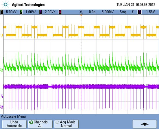
During subsequent experimentation with the code, i decided to capture the waveforms of the CLK, SIMO and SOMI pins.
The datasheet of the AD9834 states that "After FSYNC (SOMI) goes low, serial data is shifted into the input shift register of the device on the falling edges of SCLK for 16 clock pulses. FSYNC (SOMI) can be taken high after the 16th falling edge of SCLK"
Now i captured all the three signals during program execution, and this is how they look.

Top/ 1 / yellow = SIMO pin
Middle / 2 / Green = SOMI pin
Bottom / 3 / purple = CLK pin
The clk waveform looks weird to me.
I have the following doubts?
1) Does the CLK waveform look satisfactory?
2) Are my initializations correct?
3) What are the possible reasons because of which my code fails to work?
I would be eternally grateful, if someone could help me out.
PS : (I, II, III, IV and V are the 16bits of data (words) i am entering)
The Code:
#include <msp430x26x.h>
void main (void)
{
volatile unsigned int i;
WDTCTL = WDTPW+WDTHOLD; // Stop watchdog timer
BCSCTL1 = CALBC1_1MHZ; // Set DCO
DCOCTL = CALDCO_1MHZ;
for(i=2100;i>0;i--); // Wait for DCO to stabilize.
// initialization of port pins
P1DIR = 0xC0;
P1OUT = 0xC0;
P2DIR = 0x00;
P2OUT = 0x00;
P3SEL = 0x0E;
P3DIR = 0x0E;
P3OUT = 0x0E;
P5SEL = 0X0E;
P5DIR = 0x0E;
P5OUT = 0x0E;
// initialization concerned with UCBO
UCB0CTL0 |= UCMST+UCSYNC+UCCKPL+UCMSB; //3-pin, 8-bit SPI master
UCB0CTL1 |= UCSSEL_2; // SMCLK
UCB0BR0 = 0x02; // /2
UCB0BR1 = 0; //
UCB0CTL1 &= ~UCSWRST; // **Initialize USCI state machine**
IE2 |= UCB0RXIE; // Enable USCI_A0 RX interrupt
// initialization concerned with UCB1
UCB1CTL0 |= UCMST+UCSYNC+UCCKPL+UCMSB; //3-pin, 8-bit SPI master
UCB1CTL1 |= UCSSEL_2; // SMCLK
UCB1BR0 = 0x02; // /2
UCB1BR1 = 0; //
UCB1CTL1 &= ~UCSWRST; // **Initialize USCI state machine**
UC1IE |= UCB1RXIE; // Enable USCI_A0 RX interrupt
// Initialize buffers
UCB0TXBUF = 0x00;
UCB1TXBUF = 0x00;
_BIS_SR(LPM0_bits+GIE);
}
#pragma vector=USCIAB0RX_VECTOR
__interrupt void USCIA0RX_ISR (void)
{
volatile unsigned int i;
while (!(IFG2 & UCB0TXIFG)); // USCI_B0 TX buffer ready?
while (!(UC1IFG & UCB1TXIFG)); // USCI_B1 TX buffer ready?
P1OUT &= ~0xC0;
// I start
P3OUT = 0x0A;
P5OUT = 0x0A;
UCB0TXBUF = 0X21;
UCB0TXBUF = 0X00;
UCB1TXBUF = 0X21;
UCB1TXBUF = 0X00;
for(i=50;i>0;i--);
P3OUT = 0x0E;
P5OUT = 0x0E;
for(i=50;i>0;i--);
// I ends
// II start
P3OUT = 0x0A;
P5OUT = 0x0A;
UCB0TXBUF = 0X50;
UCB0TXBUF = 0XC7;
UCB1TXBUF = 0X50;
UCB1TXBUF = 0XC7;
for(i=50;i>0;i--);
P3OUT = 0x0E;
P5OUT = 0x0E;
for(i=50;i>0;i--);
// II ends
// III start
P3OUT = 0x0A;
P5OUT = 0x0A;
UCB0TXBUF = 0X40;
UCB0TXBUF = 0X00;
UCB1TXBUF = 0X40;
UCB1TXBUF = 0X00;
for(i=50;i>0;i--);
P3OUT = 0x0E;
P5OUT = 0x0E;
for(i=50;i>0;i--);
// III ends
// IV start
P3OUT = 0x0A;
P5OUT = 0x0A;
UCB0TXBUF = 0XC0;
UCB0TXBUF = 0X00;
UCB1TXBUF = 0XC0;
UCB1TXBUF = 0X00;
for(i=50;i>0;i--);
P3OUT = 0x0E;
P5OUT = 0x0E;
for(i=50;i>0;i--);
// IV ends
// V starts
P3OUT = 0x0A;
P5OUT = 0x0A;
UCB0TXBUF = 0X20;
UCB0TXBUF = 0X00;
UCB1TXBUF = 0X20;
UCB1TXBUF = 0X00;
for(i=50;i>0;i--);
P3OUT = 0x0E;
P5OUT = 0x0E;
for(i=50;i>0;i--);
// V ends
for(i=30;i>0;i--);
}

