


Part Number: LP-MSPM0C1104
Other Parts Discussed in Thread: MSPM0C1103, MSPM0C1104, , UNIFLASH
Hi Team,
I am facing a critical debug access issue with the LP-MSPM0C1104 LaunchPad after reconfiguring PA19 and PA20 as GPIO. My intention was to match the target PCB design, where the actual device is MSPM0C1103 (8-pin variant), and PA19/PA20 are required as GPIO. Based on this, I configured these pins as GPIO in my application and flashed the MSPM0C1104 LaunchPad.
Observed Behavior
-
CCS error:
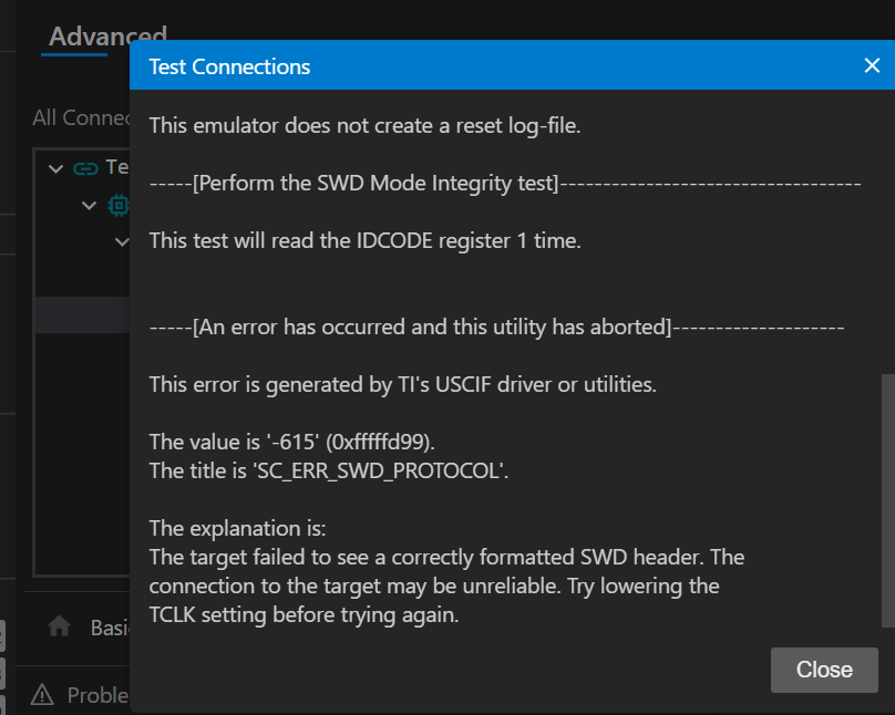
CS_DAP_0: Error connecting to the target: DAP Connection Error - SWD Test Connection:
- IDCODE read is successful only when reset button is pressed
- IDCODE =
0x6ba02477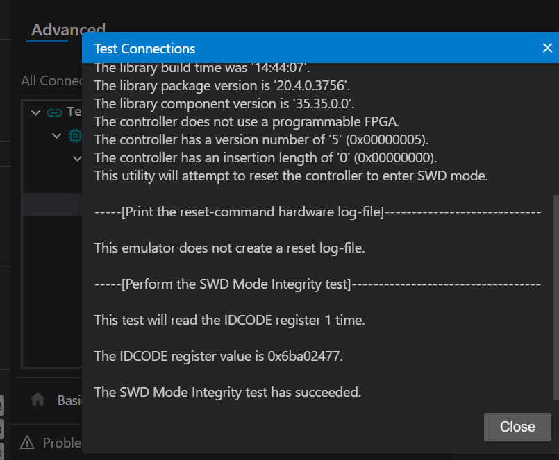
- Outside reset window → communication fails
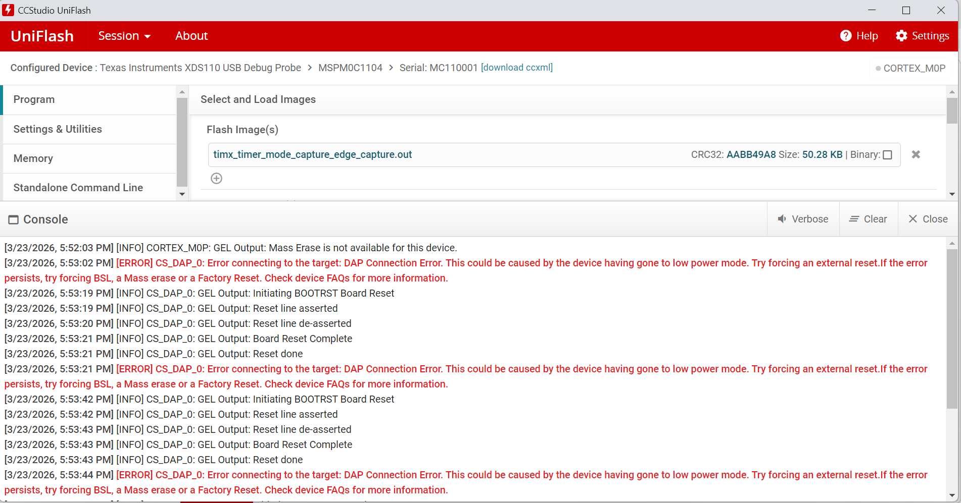
- UniFlash/GEL output:
-
Mass Erase is not available for this device - DSSM Mass Erase → fails
- DSSM Factory Reset → fail
-
- Could configuring PA19/PA20 as GPIO disable or interfere with SWD/debug access on MSPM0C1104?
- Is there a recommended way to safely use these pins as GPIO without losing debug access?
- Are there additional recovery mechanisms beyond DSSM Mass Erase / Factory Reset?
- Is this condition recoverable, or is the device effectively locked?
- How can I determine whether the issue is with U1 (target MCU) or U2 (onboard debugger/XDS110)?
- How can the MSPM0C1104 be programmed in standalone mode (without the onboard debugger)?
No intentional debug/security configuration was applied. Issue occurred immediately after flashing user application.
Any guidance on recovery or correct SWD-safe GPIO configuration would be greatly appreciated.
Regards,
Janet
