This thread has been locked.

If you have a related question, please click the "Ask a related question" button in the top right corner. The newly created question will be automatically linked to this question.

MSP430FR5869: Tharmal Pad land pattern

Part Number: MSP430FR5869

Hi,

I would like you to ask following question of MSP430FR5869 QFN package.

* According to datasheet, you recommend to use thermal via for this device as shown below.

image.png
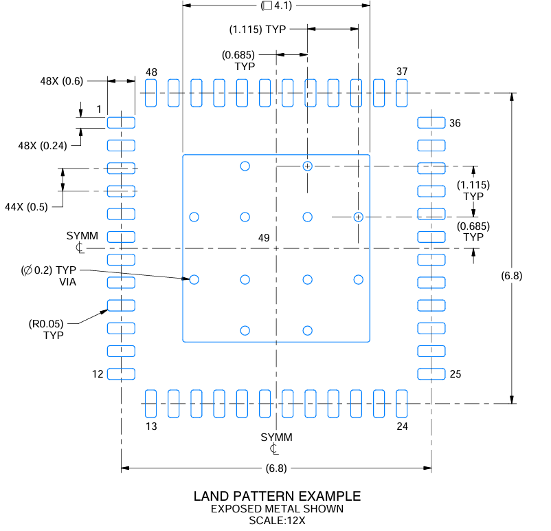
However, customer ask following question to me.
Q. Is it possible to use thermal land (not to use thermal via) ?

Actually, "FR" series is low power device, so I think that it is not mandatory requirement to use thermal via. However, do you have any information about thermal difference between with thermal pad and without thermal pad ?

Best Regards,

  • Hi,

    The thermal pad is the GND in QFN package. Generally in PCB design, we will make this pad (GND) be connected with ground in other layers by vias, and those vias also work as thermal vias. 

    Could you please share why you do not want to add vias in this GND pad in MCU QFN package?

  • Hi,

    Thank you for your reply.
    >Could you please share why you do not want to add vias in this GND pad in MCU QFN package?
    Due to issues with implementing device on their custom board.
    1. The solder does not melt easily.
    2. Generate solder ball. (Due to solder wicking)

    In previous question, I asked only situation case of changing thermal via to thremal land.
    However, if possible, please give your comment when we just decrease number of threnal vias from datasheet description.

    Best Regards,


  • It is not a mandatory requirement to achieve all the thermal vias as shown in datasheet. You could achieve/decrease the vias number according to your application requirement in PCB design.

  • Hi,

    Thank you for your reply.

    >You could achieve/decrease the vias number >according to your application requirement in >PCB design.

    Understood.

    If you have any example information about device temperature difference between thermal via numbers which follow datasheet recommendation and reducing thermal via numbers from datasheet recommendation, could you please share it to me ?

    Customer is concerned about power consumption and analog accuracy difference when they perform above change.

    If concern is only thermal difference, it is ok. But if there is any concern you have already found, could you also let me know ?

    Best Regards,

  • Hi Ryuuichi,

    Sure. You do not need to be worried so much for the reduce of vias. The thermal vias is not a mandatory requirement and should be designed according to actual PCB layout network.

  • Hi,
    Let me confirm just in case.
    >If concern is only thermal difference, it is ok. 
    For above, what I would like to confirm is that thermal pad does NOT connect to internal electric circuit. Is my understanding that thermal pad do NOT connect to any internal electric circuit correct ?

    Best Regards,

  • Whether there is a connection or not, TI recommends connecting it to Vss:

  • Hi,
    >Whether there is a connection or not, TI recommends connecting it to Vss:
    I have already understood about this.
    What I would like to confirm is "Thermal pad is connected certain INTERNAL ELECTRIC CIRCUIT" or not."
    (In other words, thermal pad is floating pin or not.)
    Could you reconfirm ?

    Best Regards,

  • Hi Ryuuichi,

    The thermal pad is not internally connected to GND network in MCU, but it is recommended to connect it to VSS in PCB design.

  • An even better note:

    Note that it does not say "electrical"

**Attention** This is a public forum