This thread has been locked.

If you have a related question, please click the "Ask a related question" button in the top right corner. The newly created question will be automatically linked to this question.

How to setup ADC to collect 512 per second using DMA through PM_TA1CCR0A and PM_TA1CCR1A port?

Other Parts Discussed in Thread: CC430F5137, SYSBIOS

Hello:

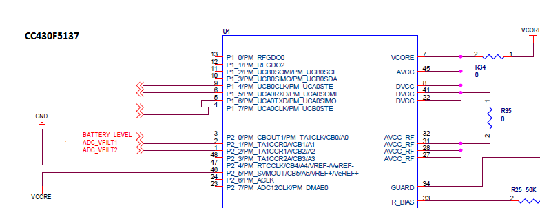
I need help to setup the CC430F5137 to read ADC value from PM_TA1CCR01 and PM_TA1CCR1A ports. The ADC must collect 512 sample per second by using DMA only.

I would like hardware / software setup:
* ADC from PM_TA1CCR0A and PM_TA1CCR1A ports
* Collect 512 samples per second
* Using only DMA


---------------------------- Sample Source Code setup -------------------

#include <msp430.h>
#include <cc430f5137.h>
#include <xdc/std.h>
#include <xdc/runtime/Log.h>
#include <ti/sysbios/BIOS.h>
#include <ti/sysbios/knl/Task.h>
#include <ti/sysbios/knl/Semaphore.h>

/* Semaphore handle defined in task.cfg */
extern const Semaphore_Handle mySem;

unsigned int DMA_DST;

/* Counter incremented by timer interrupt */
volatile UInt tickCount = 0;

/*
 *  ======== main ========
 */
Void main()
{

 WDTCTL = WDTPW+WDTHOLD;                   // Hold WDT

   P1OUT  = 0;                               // P1.0, P1.6 clear
   P1DIR |= BIT0 + BIT1 + BIT6;                     // P1.0 output to LED, P1.6 GND

   PMAPPWD = 0x02D52;                        // Get write-access to port mapping regs
   P2MAP6 = PM_TA0CCR1A;                     // Map TA0CCR1 output to P2.6
   PMAPPWD = 0;                              // Lock port mapping registers

   P2DIR |= BIT6;                            // Output TA0CCR1
   P2SEL |= BIT6;                            // Enable TA0CCR1 functionality

   /* Initialize Timer A0 */
   TA0CCR0 = 0xFFFE;
   TA0CCR1 = 0x8000;
   TA0CCTL1 = OUTMOD_3;                       // CCR1 set/reset mode
   TA0CTL = TASSEL_2+MC_1+TACLR;              // SMCLK, Up-Mode

   /* Initialize REF module */
   // Enable 2.5V shared reference, disable temperature sensor to save power
   REFCTL0 |= REFMSTR+REFVSEL_2+REFON+REFTCOFF;

   /* Initialize ADC12_A */
   ADC12CTL0 = ADC12SHT0_15+ADC12MSC+ADC12ON;// Sampling time, MSC, ADC12 on
   ADC12CTL1 = ADC12SHS_1+ADC12CONSEQ_2;     // Use sampling timer; ADC12MEM0
                                             // Sample-and-hold source = CCI0B =
                                             // TBCCR1 output
                                             // Repeated-single-channel
   ADC12MCTL0 = ADC12SREF_0+ADC12INCH_0;     // V+=AVcc V-=AVss, A0 channel
   ADC12CTL0 |= ADC12ENC;

   __delay_cycles(75);                       // ~75us shared ref. settling time

   /* Initialize DMA0 */
   DMACTL0 = DMA0TSEL_24;                    // ADC12IFGx triggered
   DMACTL4 = DMARMWDIS;                      // Read-modify-write disable
   DMA0CTL &= ~DMAIFG;
   DMA0CTL = DMADT_4+DMAEN+DMADSTINCR_3+DMAIE; // Rpt single tranfer, inc dst, Int
   DMA0SZ = 1;                               // DMA0 size = 1
   __data16_write_addr((unsigned short) &DMA0SA,(unsigned long) &ADC12MEM0);
                                             // ... from ADC12MEM0
   __data16_write_addr((unsigned short) &DMA0DA,(unsigned long) &DMA_DST);
                                             // ... to destination in RAM


    /*
     * Print "Hello world" to a log buffer.
     */
    Log_info0("Hello world\n");

    /*
     * Start BIOS.
     * Begins task scheduling.
     */
    BIOS_start();        /* does not return */
}

//------------------------------------------------------------------------------
// DMA Interrupt Service Routine
//------------------------------------------------------------------------------
void DMA_ISR_fnx(void)
{
  switch(__even_in_range(DMAIV,16))
  {
    case 0: break;
    case 2:                                 // DMA0IFG = DMA Channel 0
      P1OUT |= BIT0;                        // Toggle P1.0
      break;
    case 4: break;                          // DMA1IFG = DMA Channel 1
    case 6: break;                          // DMA2IFG = DMA Channel 2
    case 8: break;                          // DMA3IFG = DMA Channel 3
    case 10: break;                         // DMA4IFG = DMA Channel 4
    case 12: break;                         // DMA5IFG = DMA Channel 5
    case 14: break;                         // DMA6IFG = DMA Channel 6
    case 16: break;                         // DMA7IFG = DMA Channel 7
    default: break;
  }

  P1OUT &= ~BIT0;                        // Toggle P1.0

}

----------------------------------------------------------------------------------------------------------

Thank You

Mike

  • Your schematics doesn't show any connection on P2.6, so why do you configure it using the port mapping controller?

    The TA0.1 signal connection to the ADC12 (ADC12SHS_1) is internal and does not need a mapping to a port pin.

    To have a sample frequency of 512 samples per second, you'll have to set TA0CCR0 to a value that corresponds to 1/512 second.
    On a timer frequency of 1MHz (default SMCLK), this would be 1952. You set it to 65534, which gives only 15.25 loops per second.
    To have the sampling input open 50% of the time, you'll also have to set TA0CCR1 to 977.

    Mike Dawn said:
    * ADC from PM_TA1CCR0A and PM_TA1CCR1A ports

    I'm not sure what you mean by this. On this MSP, TA0.1 is the only available timer trigger  for the ADC. Other MSPs have two more, usually TB0 and TB1. And the trigger signal is connected internally, and has nothing to do with 'ports'.

  • Your schematics doesn't show any connection on P2.6, so why do you configure it using the port mapping controller?
    Answer: In this case, the SMCLK clock is need to use.

    OK, can you modify the example source codes to let me see how it work?

    Now, I have another question reguires to DMA. Can MSP430 do DMA A0, A1, and A2 in one burst?

    Mike

  • Mike Dawn said:
    Your schematics doesn't show any connection on P2.6, so why do you configure it using the port mapping controller?
    Answer: In this case, the SMCLK clock is need to use.

    Hmmm, what has SMCLK to do with mapping the only internally needed TA0CCR1A fucntionality to a port pin? Uless you want to see the TA0CCR1A signal on a scope for verification, this is completely superfluous.

    Mike Dawn said:
    Can MSP430 do DMA A0, A1, and A2 in one burst?

    No. But it can do ADC12MEM0..x in one burst. So you set up the ADC12 to copnvert a sequence, set up ADCMCTLx..y (not necessarily 0..2, as the analog channel in the ADC12MCTLx register can be freely set to any channel, any order and even multiple times or with gaps.) and configure the DMA top copy over a block from ADCMEMx to ADCMEMy when the sequence is complete.

  • Hi Jens-Michael Gross:

    OK, the IT-CC430 example source is wrong example for my application. Since, the DMA cannot do parallel transfer that I hoping for.

    I am looking at the cc430x513x_adc12_06.c that talk about the ADC12_A "Repeated Sequence of Conversions", which read in ADC value from A0, A1, and A2 etc. During reading ADC value, I also need to pack 12-bit value into packet buffer for RF transmission.

    So, here is my new ADC configuration, what do you think?

    Thank You
    Mike

    ---------------------- Setup ADC etc. -------------
    P2SEL = 0x0F;                             // Enable A/D channel inputs
      
     /* TA0CCR0 Register */
     TA0CCR0 = 8192000 / 512;
       
     /* TA0CCR1 Register */
     TA0CCR1 = TA0CCR0 / 2;
      
        TA0CCTL1 = OUTMOD_3;
      
        TA0CTL = TASSEL_2 + MC_1 + TACLR;
        
        TA0CTL = TASSEL_2 + MC_1 + TACLR;
     
     
        ADC12CTL0 = ADC12ON+ADC12MSC+ADC12SHT0_15;
     ADC12CTL1 = ADC12SHP+ADC12CONSEQ_3; 
     ADC12MCTL0 = ADC12SREF_0+ADC12INCH_0;                 // ref+=AVcc, channel = A0
     ADC12MCTL1 = ADC12SREF_0+ADC12INCH_1;                 // ref+=AVcc, channel = A1   
     ADC12MCTL2 = ADC12SREF_0+ADC12INCH_2+ADC12EOS;        // ref+=AVcc, channel = A2, end seq.
     
     ADC12IE = ADC12IE2;                        // Enable ADC12IFG.2
     ADC12CTL0 |= ADC12ENC;                    // Enable conversions
     ADC12CTL0 |= ADC12SC;                     // Start conversion - software trigger

    --------------- ADC ISR ------------

    #pragma vector=ADC12_VECTOR
    __interrupt void ADC12ISR (void)
    {
      static unsigned int index = 0;

      switch(__even_in_range(ADC12IV,34))
      {
      case  0: break;                           // Vector  0:  No interrupt
      case  2: break;                           // Vector  2:  ADC overflow
      case  4: break;                           // Vector  4:  ADC timing overflow
      case  6: break;                           // Vector  6:  ADC12IFG0
      case  8: break;                           // Vector  8:  ADC12IFG1
      case 10:                                     // Vector 10:  ADC12IFG2

        A0results[index] = ADC12MEM0;           // Move A0 results, IFG is cleared
        A1results[index] = ADC12MEM1;           // Move A1 results, IFG is cleared
        A2results[index] = ADC12MEM2;           // Move A2 results, IFG is cleared
        index++;                                // Increment results index, modulo; Set Breakpoint1 here
       
        if (index == 8) 
            index = 0;       // Reset index, Set breakpoint 2 here
         break;
      case 12: break;                            // Vector 12:  ADC12IFG3
      case 14: break;                           // Vector 14:  ADC12IFG4
      case 16: break;                           // Vector 16:  ADC12IFG5
      case 18: break;                           // Vector 18:  ADC12IFG6
      case 20: break;                           // Vector 20:  ADC12IFG7
      case 22: break;                           // Vector 22:  ADC12IFG8
      case 24: break;                           // Vector 24:  ADC12IFG9
      case 26: break;                           // Vector 26:  ADC12IFG10
      case 28: break;                           // Vector 28:  ADC12IFG11
      case 30: break;                           // Vector 30:  ADC12IFG12
      case 32: break;                           // Vector 32:  ADC12IFG13
      case 34: break;                           // Vector 34:  ADC12IFG14
      default: break;
      } 
    }


**Attention** This is a public forum