Other Parts Discussed in Thread: MSP430F2013, BQ24650
Hi
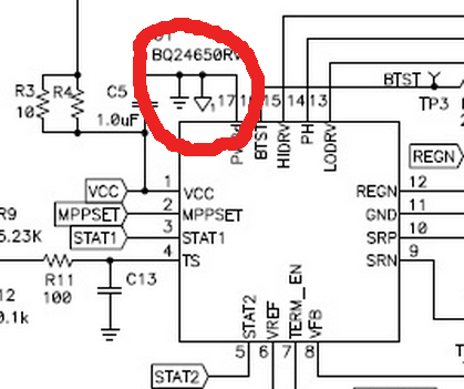
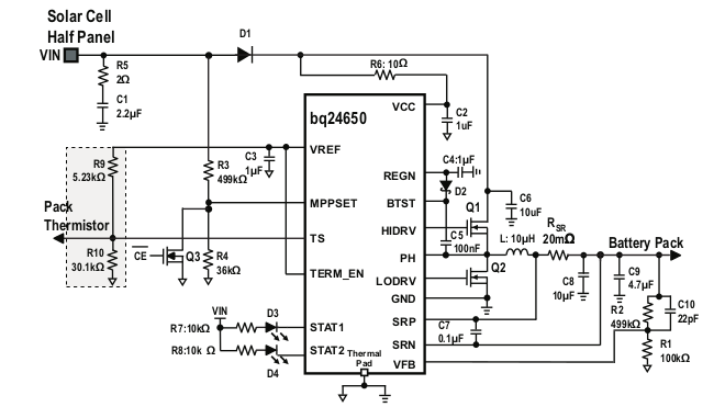
I am designing with MSP430F2013 which is been powered by TPS71501. The circuit board also has BQ24650 which requires PGND and AGND.
My question is , what do I connect as ground for the MSP430 and for the TPS71501 ??
Thanks