This thread has been locked.

If you have a related question, please click the "Ask a related question" button in the top right corner. The newly created question will be automatically linked to this question.

CC430x613x + ADXL345

Other Parts Discussed in Thread: CC430F5137, CC430F6137

Hi guys!

I saw a few topics about the msp430 + adxl345. I copied some codes and tried to run them using the kit CC430F6137RF900.

The reading byte that I've got was exactly what I sent or simply 0xFF. I think the error is on the clock configuration.

Following is the code I'm using at this moment.

Thank you in advance.

#include "cc430x613x.h"

// FUNCTION PROTOTYPES

void CONFIGURE_SPI(void);
void INITIALIZE_TIMER(void);
void ADXL_On(void);
void GET_DEVICE_ID(void);

// VARIABLE DECLARATION
unsigned char DEVID;

void CONFIGURE_SPI()
{
UCA0CTL1 |= UCSWRST;

// Configuring the IO pins for SPI
PMAPPWD = 0x02D52; // Get write-access to port mapping regs
P2MAP0 = PM_UCA0SIMO; // Map UCA0SIMO output to P2.0
P2MAP2 = PM_UCA0SOMI; // Map UCA0SOMI output to P2.2
P2MAP4 = PM_UCA0CLK; // Map UCA0CLK output to P2.4
PMAPPWD = 0; // Lock port mapping registers

P1OUT |= BIT0; // Set P1.0 for LED
P1OUT |= BIT2; // Set P1.2 for CS
// Set P1.2 for slave reset
P1DIR |= BIT2 + BIT0; // Set P1.0, P1.2 to output direction
P2DIR |= BIT0 + BIT2 + BIT4; // ACLK, MCLK, SMCLK set out to pins
P2SEL |= BIT0 + BIT2 + BIT4; // P2.0,2,4 for debugging purposes.

UCA0CTL1 |= UCSWRST; // **Put state machine in reset**
UCA0CTL0 |= UCMST+UCSYNC+UCCKPL+UCMSB+UCCKPH+UCMODE_0; // 3-pin, 8-bit SPI master
UCA0CTL0 &= ~UC7BIT;
// Clock polarity high, MSB
UCA0CTL1 = UCSSEL_2;
UCA0BR0 = 10;
UCA0BR1 = 0x00;

UCA0CTL1 &= ~UCSWRST; // **Initialize USCI state machine**

}

void ADXL_On() // Enable the chip select pin of ADXL345
{
// CS low (Enable SPI)
P1OUT &= ~BIT2;

// Delay to wait for ADXL
TA0CCR0 = 0x6FFF; // Set the value in TA0CCR0 to start the timer

while(!(TA0CTL & TAIFG)); //TAIFG flag is set when the timer Counts to TA0CCR0
TA0CTL &= ~TAIFG; //Clear the TAIFG flag

TA0CCR0 = 0x0000; //Stop the timer
}

void INITIALIZE_TIMER()
{

TA0CTL = TACLR ;
TA0CTL = (TASSEL_2 | ID_3 | MC_1);

/* TASSEL_2 = Timer A clock source select: 2 - SMCLK
ID_3 = Timer A Input Divider 3 "/8"
MC_1 = Timer A mode control - Up counter */

TA0EX0 = TAIDEX_1; // Further Dividing by 2 ;

}

void GET_DEVICE_ID()
{

ADXL_On();

UCA0IFG &= ~UCRXIFG;
while (!(UCA0IFG&UCTXIFG)); // USCI_A0 TX buffer ready?
UCA0TXBUF = 0x80; // Transmit 0x80 to get the Device ID
while (UCA0STAT & UCBUSY);
UCA0TXBUF = 0xF4; // Sending dummy variable to enable the reception
while (UCA0STAT & UCBUSY);

// Debug
DEVID = 0xAA;

DEVID = UCA0RXBUF;

// CS high (Disable SPI)
P1OUT |= BIT2 ;

}

// MAIN CLASS
int main()
{
WDTCTL = WDTPW + WDTHOLD; // STOP THE WATCHDOG TIMER
// CS low (Disable SPI)
P1OUT |= BIT2 ;
CONFIGURE_SPI();
INITIALIZE_TIMER();
// Enable SPI
UCA0CTL1 &= ~UCSWRST;

while(1) {
GET_DEVICE_ID();
P1OUT = 0x00;
if(DEVID == 0xE5){
P1OUT = 0x01; // LED is ON when the DEVID matches 0xE5(Device Id of ADXL345)
}
}

return 0;
}

  • My code uses UCRXIFG to test for the end of a transfer instead of UCBUSY. And I do a dummy read of the UCB0RXBUF to clear the interrupt after a byte transfer.

  • Artur Gontijo said:
    TA0CCR0 = 0x0000; //Stop the timer

    It doesn't stop the timer. It just causes the timer to count form 0 to 0, overflowing on each tick.
    To stop the timer, clear the MCx bits in TACTL0

    I don't know the ADxL, buit it seems wrong to wait for 1/2s (did I count the delay right?) after asserting CS before the transfer starts. usually, you assert CS right before the transfer (with a minimal setup delay of a few µs).

    However, while I hadn't used UCBUSY for waiting, the code as you wrote it should work: send 0x80, then 0xf4 (as dummy byte) and while 0xf4 is send, the answer for 0x80 is received.

    The only thing i see that could be wrong is phase and/or polarity of the clock. You should try all four combinations.

    That you get 0xf4 (what you send) back, does surprise me a bit, 0xff is what to expect when the slave refuses to answer :)

  • Thanks for the answers!

    I still trying to read the Device ID, but now with a simple code.

    #include "cc430x613x.h"

    #define SPI_On P1OUT &= ~BIT2
    #define SPI_Off P1OUT |= BIT2

    unsigned char DEVID;

    int main(){

    //turn on SPI
    WDTCTL = WDTPW + WDTHOLD; //Stop watchdog timer

    // Configuring the IO pins for SPI
    PMAPPWD = 0x02D52; // Get write-access to port mapping regs
    P2MAP0 = PM_UCA0SIMO; // Map UCA0SIMO output to P2.0
    P2MAP2 = PM_UCA0SOMI; // Map UCA0SOMI output to P2.2
    P2MAP4 = PM_UCA0CLK; // Map UCA0CLK output to P2.4
    PMAPPWD = 0; // Lock port mapping registers

    P1OUT |= BIT0; // Set P1.0 for LED
    P1OUT |= BIT2; // Set P1.2 for CS
    // Set P1.2 for slave reset
    P1DIR |= BIT2 + BIT0; // Set P1.0, P1.2 to output direction
    P2DIR |= BIT0 + BIT2 + BIT4; // Set P2.0,P2.2 and P2.4 to output direction
    P2SEL |= BIT0 + BIT2 + BIT4; // P2.0,2,4 for debugging purposes.

    UCA0CTL1 |= UCSWRST; // **Put state machine in reset**
    UCA0CTL0 |= UCMST+UCSYNC+UCCKPL+UCCKPH+UCMSB; // 3-pin, 8-bit SPI master
    // Clock polarity and phase high, MSB
    UCA0CTL1 |= UCSSEL_2; // SMCLK
    UCA0BR0 = 2; // divide by 8 (aka 1MHz SPI)
    UCA0BR1 = 0;

    UCA0CTL1 &= ~UCSWRST; //Initialize USCI state machine

    P1OUT &= ~BIT2; // Now with SPI signals initialized,
    P1OUT |= BIT2; // reset slave

    //__delay_cycles(100); // Wait for slave to initialize

    // CS Low (SPI On)
    SPI_On;

    UCA0IFG &= ~UCRXIFG;
    while (!(UCA0IFG&UCTXIFG)); // TXBUF ready?
    UCA0TXBUF = 0x00; // Request for Device ID
    while ((UCA0STAT & UCRXIFG )); // Transmission Done?

    while (!(UCA0IFG&UCTXIFG)); // TXBUF ready?
    UCA0TXBUF = 0x7E; // Transmit dummy byte
    while ((UCA0STAT & UCRXIFG )); // Transmission Done?

    // DEBUG
    DEVID = 0xFD;
    while (!(UCA0IFG & UCRXIFG)); // RXBUF ready?
    DEVID = UCA0RXBUF;
    while ((UCA0STAT & UCRXIFG )); // Transmission Done?

    // CS High (SPI Off)
    SPI_Off;

    }

    The odd thing is that when I run the program with just one breakpont at the line "DEVID = UCA0RXBUF;" the DEVID is 0x7E. But when I run it with the step by step mode the DEVID is 0x00.

    About the phase and polarity, they must be 1. From datasheet:

    "The maximum SPI clock speed is 5 MHz with 100 pF maximum loading, and the timing scheme follows clock polarity (CPOL) = 1 and clock phase (CPHA) = 1"

    I think the error still the clock or maybe I am doing wrong the pin assignments.

  • Artur Gontijo said:
    and the timing scheme follows clock polarity (CPOL) = 1 and clock phase (CPHA) = 1"

    No Motorola polarity and Ti polarity aren't the same. On MSP, polarity=1 means clock is idle-high. Following Motorola notation, polarity=0 is idle-high. To be sure, compare the timing diagrams, not the verbal description :)

    Artur Gontijo said:
    when I run it with the step by step mode the DEVID is 0x00.

    It's a common misunderstanding that a debugger allows you to to freeze the target. It does only freeze the CPU. Btu the USCI is a separate module, and the world doesn't stop turning when you hit the break button. On some MSPs, the debuger can also stop the clocks, but not on alland I'm not sure whether this is the default option.
    Try to imagine what happens if teh CPU doesn't ocntinue the code, but the USCI continues with same speed. Then aou have what happens when you single-step through your code.

  • Thanks again, Jens-Michael!

    About the polarity and the phase, the correct is PHASE= 0 and POLARITY= 1 (I saw this in a project using a MSP430 and a ADXL345).

    About the debug, now I'm only setting a breakpoint at the line with the comment:

    Samething...

    // CS Low (SPI On)
    SPI_On;
    __delay_cycles(1100);

    UCA0IFG &= ~UCRXIFG;
    while (!(UCA0IFG&UCTXIFG)); // TXBUF ready?
    UCA0TXBUF = 0x00; // Request for Device ID
    while ((UCA0STAT & UCRXIFG )); // Transmission Done?

    while (!(UCA0IFG&UCTXIFG)); // TXBUF ready?
    UCA0TXBUF = 0x7E; // Transmit dummy byte
    while ((UCA0STAT & UCRXIFG )); // Transmission Done?

    // DEBUG
    DEVID = 0xFD;
    while (!(UCA0IFG & UCRXIFG)); // RXBUF ready?
    DEVID = UCA0RXBUF;
    while ((UCA0STAT & UCRXIFG )); // Transmission Done?

    if(DEVID == 0xE5){ // Breakpoint
    P1OUT &= ~BIT0; //Turns the LED off 
    }

    // CS High (SPI Off)
    SPI_Off;

    I'm still getting the 0x7E (It must be a wrong delay. The read is too fast that is reading the byte that is being sent. Am I right?)

    I've just found this "Quick Start Guide" manual for ADXL345 - http://www.analog.com/static/imported-files/application_notes/AN-1077.pdf

    It talks about a delay of 1,1 ms (so I've put this 1100 delay) but with no success.

    Another thing that I've been thinking is about the CS, when I transmit a byte I have to pull the CS high and then low again or not?!

  • I just test with CSS and IAR and in both cases the error is the same. The same byte sent is read. =/

  • In your latest code this test probably won't work:

    UCA0STAT & UCRXIFG

  • Hey Tim,

    I tried with:

    1 - while ((UCA0STAT & UCRXIFG ));

    2 - while ((UCA0STAT & UCBUSY));

    3 - while (!(UCA0IFG & UCTXIFG));

    In different positions, all ths following another post from this forum. But when the code doesn't stuck, the byte read still the same that was sent.

  • Artur Gontijo said:
    1 - while ((UCA0STAT & UCRXIFG ));

    This cannot work because UCRXIFG isn't part of UCA0STAT,

    However, you only can read in RBUF what you wrote to TXBUF if there is a loopback of some sort. This may be that the UCLISTEN bit is set or that you have misprogrammed the port mapping. Keep in mind that the original mapping is still active (if you have more than one port pin mapped to SOMI, the USCI will receive the ORed signal from both pins). You'll have to map something else (or PM_ANALOG) to P1.6 etc to deactivate the original mapping.

  • Progress!
    With the last code I could read the device id! =)
    The problem was with my breadboard, for some reason the pins SIMO and SOMI were in "short circuited".

    BUT, when I change the sent byte to 0x30 (to receive 0x02) the change just take effect at the second execution, at the first the received byte remains the 0xE5.

    And now I'm trying to use the Vcc and GND of my board to supply the ADXL (Can I use the VRef+ and VRef- pins to do this?! But this is for other topic =P)

    Thanks guys! =)

  • The Vcc and the GND is working! =)

    Now remains this bug with the delay to receive the correct response for the sent byte.

    Artur Gontijo

  • Now I'm trying with the use of interruptions (on RX).

    #include "cc430x613x.h"

    #define SPI_On P1OUT &= ~BIT2
    #define SPI_Off P1OUT |= BIT2

    unsigned char DEVID=0x7E, addr=0x00,alvo=0x00;
    unsigned char X0=0x00, X1=0x00, Y0=0x00, Y1=0x00, Z0=0x00, Z1=0x00;

    void config_SPI(void ){

    UCA0CTL1 |= UCSWRST; // **Put state machine in reset**
    UCA0CTL0 |= UCMST+UCSYNC+UCCKPL+UCMSB; // 3-pin, 8-bit SPI master, Clock polarity high, MSB
    UCA0CTL0 &= ~UCCKPH; // Phase low

    UCA0CTL1 |= UCSSEL_2; // SMCLK
    UCA0BR0 = 0x02; // divide by 2 (aka 4MHz SPI)
    UCA0BR1 = 0x00;

    UCA0CTL1 &= ~UCSWRST; // Initialize USCI state machine

    UCA0IE |= UCRXIE; // Enable USCI_A0 RX interrupt

    }

    void main(void)
    {

    WDTCTL = WDTPW + WDTHOLD; //Stop watchdog timer

    // Configuring the IO pins for SPI
    PMAPPWD = 0x02D52; // Get write-access to port mapping regs
    P2MAP0 = PM_UCA0SIMO; // Map UCA0SIMO output to P2.0
    P2MAP1 = PM_UCA0SOMI; // Map UCA0SOMI output to P2.1
    P2MAP2 = PM_UCA0CLK; // Map UCA0CLK output to P2.2
    PMAPPWD = 0; // Lock port mapping registers

    P2OUT &= ~BIT4; // Set P2.4 (GND) Low
    P2OUT |= BIT5; // Set P2.5 (Vcc) High
    P2DIR |= BIT4 + BIT5; // Set P2.4 VRef- and P2.5 VRef+ (Output)

    P1OUT |= BIT0; // Set P1.0 for LED
    //P1OUT |= BIT2; // Set P1.2 for CS
    P1DIR |= BIT2 + BIT0; // Set P1.0, P1.2 to output direction

    P2DIR |= BIT0 + BIT2; // Set P2.0 and P2.2 to output direction
    P2DIR &= ~BIT1;
    P2SEL |= BIT0 + BIT1 + BIT2; // P2.0,1,2 for debugging purposes.

    P2OUT &= ~BIT5;
    __delay_cycles(5000);
    P2OUT |= BIT5;

    config_SPI();

    SPI_On;
    __delay_cycles(5000); // Wait for slave to initialize

    addr=0x00;
    alvo=0xE5;

    while (!(UCA0IFG&UCTXIFG)); // USCI_A0 TX buffer ready?
    UCA0TXBUF = addr; // Transmit first character

    __bis_SR_register(LPM0_bits + GIE); // CPU off, enable interrupts
    }

    #pragma vector=USCI_A0_VECTOR
    __interrupt void USCI_A0_ISR(void)
    {
    switch(__even_in_range(UCA0IV,4))
    {
    case 0: break; // Vector 0 - no interrupt
    case 2: // Vector 2 - RXIFG
    while (!(UCA0IFG&UCTXIFG)); // USCI_A0 TX buffer ready?

    if (UCA0RXBUF==alvo) // Test for correct character RX'd
    P1OUT |= 0x01; // If correct, light LED
    else
    P1OUT &= ~0x01; // If incorrect, clear LED

    UCA0TXBUF = addr; // Send next value

    __delay_cycles(40); // Add time between transmissions to
    // make sure slave can process information

    SPI_Off;
    __delay_cycles(5000);
    SPI_On;
    __delay_cycles(5000); // Wait for slave to initialize

    break;
    case 4: break; // Vector 4 - TXIFG
    default: break;
    }
    }

    But the delay (error) remains. With this delay I cant be sure that the config bytes are really setting the ADXL345. So I'm stuck in this part of the project =/.

  • Artur Gontijo said:
    But the delay (error) remains. With this delay I cant be sure that the config bytes are really setting the ADXL345.

    With SPI Receive and Transmit operations operate concurrently. That means to read the ADXL345 DEVID register the sequence is:

    a) Set CS low (SPI_on)

    b) Write the DEVID register address 0x00 to UCA0TXBUF.

    c) Wait for a RXIFG. Read UCA0RXBUF, and discard the result as the output from the ADXL345 is undefined during the sending of the address byte.

    d) Write a dummy byte to UCA0TXBUF, to cause the ADXL345 to output the contents of the DEVID register.

    e) Wait for a RXIFG. Read UCA0RXBUF, which should be the contents of the DEVID register (0xE5).

    f) Set CS high (SPI_off)

    The posted code doesn't seem to follow this sequence.

  • Hey Chester,

    Thanks for the answer.

    I tryed with this code (following yours instructions):

    unsigned char read_byte(char addr){

    unsigned char RX_byte=0x00;

    //a)

    SPI_On;
    __delay_cycles(5000);

    //b)
    UCA0TXBUF = addr;

    //c)
    wait_rx;
    RX_byte = UCA0RXBUF;

    //d)
    UCA0TXBUF = 0x7E;

    //e)
    wait_rx;
    RX_byte = UCA0RXBUF;

    //f)

    SPI_Off;

    return RX_byte;

    }

    ...

    No success! When I transmit the 0x00 in a first time the answer is 0x00. In a second execution the answer is a 0xE5. The delay remains.

    I'm studying the USCI of the CC430 and the SPI of ADXL345 to seek for the explanation.

    My configration fuction for the SPI is:

    void config_SPI(void ){

    UCA0CTL1 |= UCSWRST; // **Put state machine in reset**
    UCA0CTL0 |= UCMST+UCSYNC+UCCKPL+UCMSB; // 3-pin, 8-bit SPI master, Clock polarity high, MSB
    UCA0CTL0 &= ~UCCKPH; // Phase low

    UCA0CTL1 |= UCSSEL_2; // SMCLK
    UCA0BR0 = 0x02; // divide by 2 (aka 4MHz SPI)
    UCA0BR1 = 0x00;

    UCA0CTL1 &= ~UCSWRST; // Initialize USCI state machine

    }

  • Artur Gontijo said:
    When I transmit the 0x00 in a first time the answer is 0x00. In a second execution the answer is a 0xE5. The delay remains.

    Can you clarify if you mean either:

    1. The first time you call read_byte it returns 0x00, and the second time you call read_byte it returns 0xE5.

    2.At step c) in read_byte the value read from UCA0RXBUF is 0x00, and at step e) the value read from UCA0RXBUF is 0xE5. This the expected operation, since for SPI for each byte in a transaction there is a value written to UCA0TXBUF and read from UCA0RXBUF.

    When reading from a ADXL345 register:

    - For the 1st address data byte SIMO from the CC430F613x to ADXL345 is valid, and the SOMI from the ADXL345 to CC430F613x is undefined.

    - For the 2nd data byte SIMO from the CC430F613x to ADXL345 is undefined, and the SOMI from the ADXL345 to CC430F613x contains the ADXL345 register value read.

     The following from the ADXL345 datasheet illustrates this, where X is undefined:


  • Let me try to explain.

    My code just call read_byte(addr); one time.

    When I execute the whole code (using CSS or IAR) with addr=0x00, the answer is 0x00.

    Then I terminate the program and start it again (with addr=0x00), at this time the answer is 0xE5.

    If I change the addr to 0x30 (answer 0x02), it happens again. The first execution it returns 0xE5 and at the second execution it returns 0x02.

    I think that something about buffer (of the debugger or CC430) is compromising the answer.

    Thanks.

  • Artur Gontijo said:
    I think that something about buffer (of the debugger or CC430) is compromising the answer.

    OK, I now understand the problem.

    From reading the ADXL345 data sheet when CS is high it may operate in I2C mode if what appears to be an I2C start operation appears on the SDA/SDI/SDIO and SCL/SCLK pins .

    When you load the program using CCS or IAR the CC430F613x pins will be tri-stated until your program starts running and configures the pins used to communicate with the ADXL345 in SPI mode. The ADXL345 may see edges which put it an indeterminate communication state. Adding the following before the first communication with the ADXL345 may get it into a known state:

    a. Configure SPI

    b. Set CS high. Wait at least 2.5us (minimum I2C clock period)

    c. Set CS low. Wait at least 2.5us. This should force SPI mode.

    d. Set CS high. Wait at least 2.5us 

    e. Now call read_byte

  • Thanks again Chester!

    Here go my code, if you have time, please take a look for me.

    I tryed with more delay and the result is the same...the delay remains.

    /*
     * main.c
     *
     *  Created on: 18/09/2012
     *      Author: gontijo
     */
    
    #include "cc430x613x.h"
    
    #define SPI_On P1OUT &= ~BIT2
    #define SPI_Off P1OUT |= BIT2
    
    #define wait_tx while (!(UCA0IFG & UCTXIFG))           	// TXBUF ready?
    #define wait_rx while (!(UCA0IFG & UCRXIFG))           	// RXBUF ready?
    #define wait_tm while ((UCA0STAT & UCBUSY))          	// Transmission Done?
    #define wait_or	while ((UCA0STAT & UCOE))				// Wait for overrun 0
    
    unsigned char DEVID=0x7E, addr=0x00,target=0x00;
    
    unsigned char read_byte(char addr){
    
    	unsigned char RX_byte=0x00;
    
    	SPI_On;
    	__delay_cycles(5000);
    
    	//a)
    	UCA0TXBUF = addr;
    
    	//b)
    	wait_rx;
    	RX_byte = UCA0RXBUF;
    
    	//c)
    	UCA0TXBUF = 0x7E;
    
    	//d)
    	wait_rx;
    	RX_byte = UCA0RXBUF;
    
    	SPI_Off;
    
    	return RX_byte;
    
    }
    
    void config_SPI(void ){
    
    	UCA0CTL1 |= UCSWRST;                      			// **Put state machine in reset**
    	UCA0CTL0 |= UCMST+UCSYNC+UCCKPL+UCMSB;				// 3-pin, 8-bit SPI master, Clock polarity high, MSB
    	UCA0CTL0 &= ~UCCKPH;								// Phase low
    
    	UCA0MCTL = 0;                             			// No modulation
    
    	UCA0CTL1 |= UCSSEL_2;                				// SMCLK
    	UCA0BR0 = 0x02;                        				// divide by 2 (aka 4MHz SPI)
    	UCA0BR1 = 0x00;
    
    	UCA0CTL1 &= ~UCSWRST;                				// Initialize USCI state machine
    
    }
    
    int main(){
    
    	WDTCTL = WDTPW + WDTHOLD;            				//Stop watchdog timer
    
    	// Configuring the IO pins for SPI
    	PMAPPWD = 0x02D52;                        			// Get write-access to port mapping regs
    	P2MAP0 = PM_UCA0SIMO;                     			// Map UCA0SIMO output to P2.0
    	P2MAP1 = PM_UCA0SOMI;                    			// Map UCA0SOMI output to P2.1
    	P2MAP2 = PM_UCA0CLK;                      			// Map UCA0CLK output to P2.2
    	PMAPPWD = 0;                              			// Lock port mapping registers
    
    	P2DIR |= BIT0 + BIT2;     							// Set P2.0 and P2.2 to output direction
    	P2DIR &= ~BIT1;
    	P2SEL |= BIT0 + BIT1 + BIT2;              			// P2.0,1,2 for debugging purposes.
    
    	P2OUT &= ~BIT4;
    	P2OUT &= ~BIT5;
    	P2DIR |= BIT4 + BIT5;                     			// Set P2.4 VRef- and P2.5 VRef+ (Output)
    
    	config_SPI();
    	
    	__delay_cycles(5000);								// Before power on ADXL345
    
    	P2OUT &= ~BIT4;										// Set P2.4 (GND) Low
    	P2OUT |= BIT5;										// Set P2.5 (Vcc) High
    
    	P1OUT |= BIT0;                            			// Set P1.0 for LED
    	P1DIR |= BIT2 + BIT0;                     			// Set P1.0, P1.2 to output direction
    
    	P1OUT |= BIT2;                            			// Set P1.2 for CS
    	__delay_cycles(5);
    
    	P1OUT &= ~BIT2;
    	__delay_cycles(5);
    
    	P1OUT |= BIT2;
    	__delay_cycles(5);
    
    	addr = 0x00;
    	target = 0xE5;
    
    	DEVID = read_byte(addr);
    
    	if(DEVID == target){
    		P1OUT &= ~BIT0;
    	}
    
    	return 0;
    
    }
    

    I'm trying to debug the flags of USCI, but all seems ok.

  • Chester, I found something strange now.

    if I call the read_byte() more then one time, the UCA0IFG sets the RX flag but the RXBUF remains the same!

    The RXBUF only changes when I terminate the execution and start it again. Now I'm really lost.

  • Artur Gontijo said:
    Here go my code, if you have time, please take a look for me.

    I can't see anything wrong in the code. I ran the code on a CC430F5137 with an external loopback between P2.0 (UCA0SIMO) and P2.1 (UCA0SOMI) and the result from read_byte was as expected, even when called multiple times.

    (I did find that an Olimex MSP430-JTAG-TINY-V2 can't read the first 256 bytes of RAM from 0x1C00 - 0x1CFF in a CC430F5137 which is where the global variable DEVID was placed, but a MSP-FET430UIF can)

  • I also did this test and everything seems ok.

    I'll try to configure the 4-Wire SPI now, setting CS (of ADXL) at the STE of CC430.

    Thanks Chester.

  • Chester,

    I saw this pin assignments at this Datasheet http://www.ti.com/lit/ds/slas554f/slas554f.pdf

    P1.5/PM_UCA0RXD/PM_UCA0SOMI/R23 3 46 PJ.0/TDO
    P1.6/PM_UCA0TXD/PM_UCA0SIMO/R13/LCDREF 2 47 PJ.1/TDI/TCLK
    P1.7/PM_UCA0CLK/PM_UCB0STE/R03

    But in the example code "C430F613x Demo - USCI_A0, SPI 3-Wire Master Incremented Data" the pin assignmets are:

    PMAPPWD = 0x02D52; // Get write-access to port mapping regs
    P2MAP0 = PM_UCA0SIMO; // Map UCA0SIMO output to P2.0
    P2MAP2 = PM_UCA0SOMI; // Map UCA0SOMI output to P2.2
    P2MAP4 = PM_UCA0CLK; // Map UCA0CLK output to P2.4
    PMAPPWD = 0; // Lock port mapping registers

    Can I use the port 2 to do the comunication or I only can use the port 1?

  • Artur Gontijo said:
    Can I use the port 2 to do the comunication or I only can use the port 1?

    The port 1 settings in the datasheet are the default mappings at reset.

    Port 2 can be used to do the communication, by writing to the port mapping registers as your code does.

    Can you clarify how the ADXL345 is connected to the CC430F613x, including how the ADXL345 is powered?

  • It's not a goooood schematic, but here it goes! =)

  • The pin 2.5 is the VRef+ and the pin 2.4 is the Vref-.

    The voltage between them is 3.07V (i checked with a multimeter).

  • The ADXL345 datasheet shows the ADXL345 has two supply pins:

    - VDD I/O (Digital Interface Supply Voltage)

    - VS (Supply Voltage)

    From the schematic it is not clear is P2.5 is connected to the ADXL345 VDD I/O and/or VS

  • I saw that the register DATA_FORMAT has a bit called SPI bit. The discription:

    I'm trying to set this register with the value 0x0B or 0x4B. But with the delay I'm having no success.

    Even when I run the program two or more times I read only 0x00 at this register address (0x31). After trying to write this register.

  • From the ADXL345 datasheet there are two supply pins:

    - VDD I/O (Digital Interface Supply Voltage)

    - VS (Supply Voltage)

     From you schematic it is not clear if P2.5 is connected to the ADXL345 VDD I/O and/or VS supply voltage.

    Also, why are both VCC and GND on the ADXL345 connected to I/O pins on the CC430F613x? If the CC430F613x set P2.5 low and P2.4 high that would reverse bias the ADXL345 probably causing permanent damage.

    (My previous post got stuck awaiting moderator approval, trying again....)

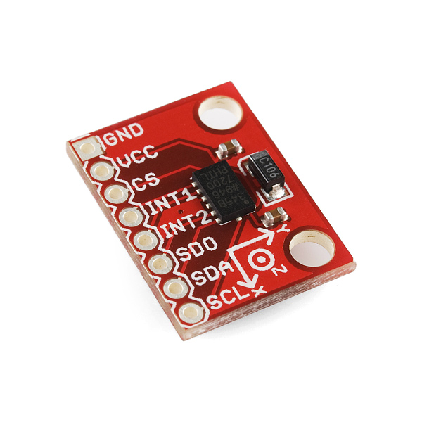
  • My ADXL board is this one https://dlnmh9ip6v2uc.cloudfront.net/images/products/9/8/3/6/09836-_01c.jpg

    So, I can only access this pins.

    About the GND, Is better connect it to the battery GND? I made like the schematic because of the distance in my arrangement.

    Thanks.

  • I would suggest connecting power and ground of the ADXL345 board directly to power and  ground of the CC430 board. Tha would reduce the number of pins you need to control. Also, using a GPIO pin as ground may be problematical because the pin may not be true ground. So the ADXL345 ends up with an offset ground and may have communication issues.

  • Hi Timothy,

    I just did what you suggested, but the delay remains the same. I noticed that the RXBUF only updates when I terminate the execution and start it again. If I call read_byte(addr) multiple times (with differents addr) the RXBUF remains the same.

    Now I'm studying and testing different clocks and baud rates.
    Thanks for help.

  • Working with other clocks and baud rates I saw that the changes in the USCI config just take effect at the second execution of the modified code. So the delay is not provided by the ADXL. Very weird.

  • I found the error!

    I supply the ADXL345 with more voltage (3.3V) and it's work perfectly.

    But now, I have to supply it with the CC430, to go on with my project. But all I got is 3.07V, Is there a way to get 3.3V from CC430F6137 or I'll have to add another battery just for the accelerometer?

    Thanks.

  • According to the ADXL345 data sheet, the part should work fine at 3V. The data sheet specifies a minimum voltage of 2.5V for a power supply > 2.5V whic should be good enough for the CC430 to use. When you have the SDXL345 connected to the cc430 board, can you measure the level of the power supplied to the ADXL345 directly?

  • With the MSP-FET430UIF plugged I can provide ~3.07V to the ADXL345. In this case I only get one value at the RXBUF (it remains the same during all the execution, no matter how many times I call the read_byte() function). I saw a project envolving the ADXL345 (same board that I have) with an arduino that provides a 3.3V to the accelerometer, so I tried with more voltage and seems to be working.
    Maybe the cause is the baud rate of the SPI, just a guess.

  • Maybe it's not the supply voltage but rather a problem with other signals, pull-ups, control lines etc which do not reach required 'high' state or are considered high with 3V but low with 3.3V, since the input logic thresholds shift with supply voltage.

    You should measure signal levels with a scope (not with a logic analyzer, which has its own thresholds and will give erroneous results if analyzer and real hardware interpret voltage levels differently)

  • Hello Artur,

    Did you manage to get this working? 

    I have been reading through your posts and I am experiencing the same behaviour with my ADXL345 and MSP430 microcontroller. 

    I have to run the program twice before I can get the result I am looking for. I also noticed that if I remove the power from the ADXL345 then press the debug button, replace the power, then run the code, that I would get a result the first time. 

    Please let me know how you got on. Thanks,

    Alex

  • Hello Alex,

    My best results were got with running the code without a debug interface (just writing the ADXL345 results to the Flash). The voltage of CC430 + ADXL345 was supplied by the same 3.3V battery. But I've noticed some delays, so I made a function to test the consistence of the results. Then I gave up on ADXL and now I'm working with CM3000-D01 (this one is very powerfull and works with 3.0V, but it is more expensive too =/ )

    I still have the ADXL here, let's keep talking about it. Let me know about your progress.

    Artur Gontijo

  • Hi Artur,

    Thanks for getting back to me. I will let you know when I figure something out. Hopefully someone in the forum might have some idea as to what is going on with the debugging causing problems.

    As far as I can tell from the oscilloscope, when the debugger is started all the pins fluctuate in some way, so I'm guessing this is what causes the troubles. If the ADXL345 is powered down for this then it seams to work, again, as far as I can tell. 

    Alex

**Attention** This is a public forum