This thread has been locked.

If you have a related question, please click the "Ask a related question" button in the top right corner. The newly created question will be automatically linked to this question.

MSP430G2553 P2.6 and P2.7 as OUTPUT

Other Parts Discussed in Thread: MSP430F2002

I am trying to declare P2.6 and P2.7 as output

I am doing the following

P2DIR |= BIT6;           
   P2DIR |= BIT7;

and I am trying to write a 1 or a 0 on them as follows

P2OUT &= ~BIT6;
P2OUT |= BIT7;

or

P2OUT &= ~BIT7;
P2OUT |= BIT6;

Is not working. Does anyone has a suggestion why it not be working?

Should I dissable something going on in the pins..?

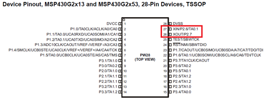
Are those pins used as something else as default?

Regards,

Daniel Hercules

  • Hey Daniel,

    It looks like for that MSP, pin 2.6 and 2.7 do share function with Xin and Xout which are used when using an external crystal.  If there isn't a crystal connected, and you just want to use them as GPIO's, you probably only have to make sure the PxSEL register is cleared.

    Thanks,

    JD

  • Thank you so much for the response...

    I know little of code,, how do I clear that?

    Like this????

    P2SEL = BIT6;

    P2SEL = BIT7;

    Daniel Hercules

  • You can clear the SEL bits the same way as you cleared the DIR bits.


    P2SEL &= ~BIT6;

    P2SEL &= ~BIT7; 


    regards Niki 

  • Thanks Niki..

    so, just a random question... if a pin in a MCU is useful for more than one thing... a.k.a  xtal, or tx or rx or something like that, I can clear whatever other function using PSEL and use that specific pin as a GPIO?

    thansk

  • In the device datasheet you can see how to set the PxDIR.x and PxSEL.x bits to select the specific function.


    If you clear the PxSEL.x bit the pin is GPIO.


    Regards,


    Niki 

  • Thank you so much

  • Yes, but ...

    You should check the data-sheet "Port Schematics" Section to find out how to set up each pin. There are a lot of exceptions to the rule you suggested.

  • Correct.

    On this MSP, clearing the bits sets it as GPIO. But, as OCY mentioned, this is not a universal statement.  Usually, when the GPIO SEL bit is cleared, the pin is it's "primary" function, not necessarily GPIO.  Looking at the "Port Schematics" section will show you how to access all the pin functions. 

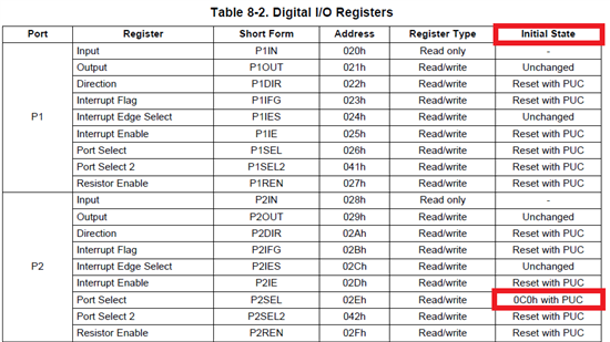
    I also wanted to point out where it's defined that these default to the ocsillator instead of GPIO.  I knew they did but took me a minute to find where in the datasheet it showed it.  Notice, that the initial state of the P2SEL register is 0xC0 which is setting those bits.

    Thanks,

    JD

  • Sorry for the dumb questions... I remind you that I am new on this..

    what is 0Xc0? does this means is oscillator by default? or what does it mean?

    what is PUC?

    Thanks

  • Hey Daniel,

    Your still learning, that's fine. 

    0x <- This means a Hex number, or a hexidecimal number. 0b <- this means a Binary number.  Set = 1 and Clear = 0;

    0xC0 = 0b 1100 0000.  Since PxSEL is an 8 bit register, you can see the top two bits are set (Bit 7 and Bit 6).


    When you use the Bit7 and Bit6 masks, what your really doing is working with individual bits:

    Bit7 = 0x80 = 0b 1000 0000

    Bit6 = 0x40 = 0b 0100 0000


    When you use the ~ (not) operator, your inverting the bits:

    ~Bit7 = 0xEF = 0b 0111 1111

    ~Bit6 = 0xBF = 0b 1011 1111


    &= is Add equals

    |= is Or equals


    Thanks,

    JD

  • Hello JD,

    I have problem setting P2.6 and P2.7 of MSP430F2002 to "low" - they always have residual voltage of 1.9V with 3.6V power supply.

    P2DIR |= 0xC0;
    P2SEL |= 0x00;
    P2REN |= 0xC0;
    P2OUT = 0x00;

    Thank you,

    IR

  • Igor Radutnuy said:
    P2SEL |= 0x00;

    This instruction sets all bits in P2SEL which are already set or are set in 0x00. Since 0x00 doesn't have any bits set, P2SEL remains unchanged. An OR instruciton cannot clear any bits at all.
    If you want to clear the bits, you need to do
    P2SEL &= ~(0xC0);
    to clear only bit 6+7 and leafe the others untouched, or do
    P2SEL = 0x00;
    to clear all bits.

  • After more investigations seems like it is the hardware issue. P1.3,4,5,6 and P2.6,7 were driving LEDs in series with 3.3k for debugging purpose. P1 has no issue driving LEDs, however P2 got residual voltage when set to low. Problem goes away when P2.6,7 drive CMOS or oscilloscope probe. Datasheet does not separate driving capability between P1 and P2.

    Than you for above advises. 

  • Please read again what we wrote about P2.6 and P2.7: the default setting is Quartz driving operation, not GPIO. You need to clear P2SEL.6 and P2SEL.7 to switch the pins to GPIO mode. Which your code didn't because you used the wrong operator.

    The residual voltage you're seeing is from the quarts oscillator drive which is desparately trying to make a (non-existing) crystal oscillate.

  • P2.6,7 work (nothing to do with wrong operator, low near VSS and high near VDD) with high impedance (CMOS inputs, oscilloscope probe) loads, however P2.6,7 cannot sink current to drive red LED in series with 3.3k (VDD=3.6V) like P1 port does. 

    If P2 was configured wrong ( for crystal oscillator), pins would not toggle between 3.6V and 1.9V (residual voltage) but stay at crystal oscillator bias voltage.

    MSP430F2002 P1/P2 ports loading capability difference not reflected in datasheet.  

  • Igor Radutnuy said:
    If P2 was configured wrong ( for crystal oscillator), pins would not toggle between 3.6V and 1.9V (residual voltage) but stay at crystal oscillator bias voltage.

    That's a valid assumption at first glance, but the (rather complex) port pin schematics tells that there are some conditions where this assumtion is wrong.

    However, the facts remain:

    1) P2SEL.6 and P2SEL.7 are SET at power on.
    2) P2SEL.6 (not necessarily P2SEL.7) need to be clear to put both pins into GPIO mode
    3) your software doesn't clear them, because the instruction you use does nothing as it uses the wrong operand and/or operator.
    4) the pins are still in oscillator mode.

    So why do you see a change on the pin on high-impdance load? because you enabled the pullup resistor, so you are pulling the pin up or down through the pullup resistor while it is still in oscillator mode. Since the oscillator driver has a much reduced driving strength at default power-on settings, the pullup resitor is stronger if there is no additional load.

    If you had just tried to properly clear the P2SEL bits as suggested, instead of assuming hardware or even silicon bugs and bad documentation, you had it already running yesterday.

  • Thank you, there were wrong operator and pull up resistors combination.

    Working code is:

    P2DIR |= 0xC0;                            // P2.6,7 outputs

    P2SEL &= ~(0xC0);                     // P2.6,7 IO option

    //P2SEL = 0x00;                           // also works to reset P2SEL bits

    //P2REN |= 0xC0;                         // P2.6,7 pullup - mistake causing problem even with properly P2SEL reset

     P2OUT = 0x00;                            // P2.6,7 reset

  • void main()
    {
        WDTCTL = WDTPW + WDTHOLD;
        P2SEL = 0;
        P2SEL2 = 0;
        P2DIR = 0XFF;
        P1DIR = 0XFF;
        while(1)
        {   

    P2DIR |= BIT6;           
       P2DIR |= BIT7;

    }

  • thank you THINH LE PHUOC

    void main()
    {
        WDTCTL = WDTPW + WDTHOLD;
        P2SEL = 0;
        P2SEL2 = 0;
        P2DIR = 0XFF;
        P1DIR = 0XFF;
        while(1)
        {   

    P2DIR |= BIT6;           
       P2DIR |= BIT7;

    }

    So, If I do it like that, I only have to declare it at the beginning of the code and that is it correct? the port behaves as I/O the whole time right?

    Thanks for the help, 

    Daniel Hercules

  • Daniel Hercules said:
    So, If I do it like that, I only have to declare it at the beginning of the code and that is it correct? the port behaves as I/O the whole time right?

    I'm not quite sure the code does what it i sintended to do.

    Dirst, it switches XT1IN and XT1OUT on P2.6/7 into GPIO mode.

    Then it turns all port pisn o fP1 and P2 into outputs. And since PxOUT is 0x00 on power-on, they are low outputs. I'm not sure this is intentional.

    And the while loop makes no sense at all. It once more sets P2.6 adn P2.7 to ouput (which they already are due to P2DIX = 0xFF) and repeats this over and over again, effectively doing nothing. (and isn't there a closing bracket missing?)

  • With Assembler you have the Bis and Bic to nicely do the intended or/andn.
    This is what my code does once in the beginning to use 2.6 and 2.7 as GPIO
             

                bic.b   #1<<6,&P2SEL            ; P2.6 set as generic pin
                bis.b   #1<<6,&P2DIR            ; P2.6 nChipSelect as output
                bis.b   #1<<6,&P2OUT            ; P2.6 nChipSelect high =off      

                bic.b   #1<<7,&P2SEL            ; P2.7 set as generic pin
                bic.b   #1<<7,&P2DIR            ; P2.7 Wlan "nIRQ" as input
                bis.b   #1<<7,&P2REN            ; P2.7 Pull Resistor
                bis.b   #1<<7,&P2OUT            ; P2.7 Make it pull-up

    I like to use #1<<6,&P2SEL etc., as I can see that I'm referring to P2.6  
    Once you have pins figured out, you could merge them to a mov.b #0x__ to save flash space if you really want too.
  • BIS(.b/w) #A,&B is equal to B|=A;
    BIC(.b/w) #1,&B is equal to B&=~(A);
    In fact, the compiler usually directly translate the latter into the former.

    So the availability of BIS and BIC is no argument for using assembler instead of C :)

    I agree on the usage of 1<<x for bits. Alternatively, you can use the BITx constants form the C headers, which also make clear what's going on. :)

    However, BIC and BIS can handle mutiple bits at the same time, so you can do

    bic.b #(1<<6+1<<7),&P2SEL (note that '+' is used. I don't know whether the assembler supports '|' in numerical expressions. C is more flexible here.

  • According to the documentation, TI's assembler does support bitwise and, or and xor. It also supports binary constants with a "b" suffix, so that makes it more flexible than C ;)

**Attention** This is a public forum