


uC: MSP430AFE253
Slave: MPL115A1 (Freescale Barometric Pressure Cell)
Assumption: The SPI mode of communications is the same for TX & RX for the slave, i.e. one should not have to change CKPH and CKPL registers of the MSP to perform a proper input shift register phase.
Issue:
SPI sends slave correct READ/WRITE address according to logic analyzer, the response from the slave reads the same as a Freescale demo board according to the logic analyzer. But, it appears that the MSPs U0RXBUF does not have the bit-0 shifted in.
Example:
Logic analyzer reads two registers in sequence as 0x77 and 0x40 (MISO).
MSP U0RXBUF reads the following, 0x3B and 0x20.
0x77 = 111 0111
0x3B = 111 011 < Missing last bit
Attached Screen Shot (data not same as above example, first line MISO, second MOSI, CLOCK, SC:
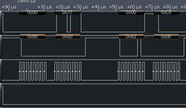
0x40 = 100 0000
0x20 = 100 000 < Missing last bit
Code:
(Note, for your reading pleasure I put in the commented out statements which are my attempts to resolve the problem, including the DO/WHILE statements to read the U0RXBUF, I stored the example variables found above in variables R & T in the below switch statements 2 & 3. Both methods store the same value. Also, using the RX_ISR produces the same results, omitted these settings, the function is self contained when called)
P1DIR = 0xA1;
//P1.5 output SPI (SIMO)
//P1.6 input SPI (SOMI)
//P1.7 output SPI (CLOCK)
P1OUT = 0x66;// IN/ Out SPI high state (attempt to alter state of line, no change)
P1SEL = 0xE0;
//P1.5 SPI - COM
//P1.6 SPI - COM
//P1.7 SPI - COM
P1SEL2 = 0x00;//P1.0
P2DIR = 0xc1;//P2.0 Output SPI CS Line
P2OUT = 0x01;//P2.0 SPI CS line high
P2SEL = 0x00;//P2.0 SPI CS line (with P2.0=1 setting, the CS line has to have the pull-up/down resistor enabled)
P2IE = 0x00;//P2.0 Make sure P2 interrupts off.
//*********************************************************************************
// 350) Enable USART0.
//*********************************************************************************
U0CTL &= ~SWRST;//
U0CTL |= CHAR + SYNC + MM; // SPI mode + 8-bit data + SPI Master
U0TCTL |= CKPH + SSEL0 + SSEL1 + STC;// See datasheet pg 517 for SPI clock and shift register settings + SMCLK clock + 3-pin SPI mode -- manual toggle of CS line.
U0BR0 = 0x02;//
U0BR1 = 0; //
U0MCTL = 0;//SPI MODE must be 0, will not work for RS-232
ME1 |= UTXE0 + URXE0;// Enabled USART0 TXD/RXD
IE1 |= URXIE0 + NMIIE;
//Below function is called for read at appropriate timing, for now 1Hz period:
void SPI_COM_Data (void)
{
//U0CTL |= LISTEN;//Feed the TX signal back into the RX (Stopped RX)
//U0CTL &= ~SYNC;//(Does not TX in this mode)
//U0CTL &= ~CHAR;// 7-bit data mode (Gets confused, incorrect after first TX)
//U0TCTL &= ~STC;//4-bin SPI mode (does not work)
switch (SPIf)
{
//4042 Send READ command
case 0:
{
P2OUT &= ~0x01;//P2.0 SPI CS line low
U0TXBUF = 0x24;//Load buffer with WRITE + CONVERT reg. address
U0TXBUF = 0x00;
__delay_cycles(37);//
P2OUT |= 0x01;//P2.0 SPI CS line High
}//CLOSE CASE 0
break;
//4042
case 1:
{
P2OUT &= ~0x01;//P2.0 SPI CS line low
//4044 Reload buffer to READ pressure MSB
U0TXBUF = 0x80;//REG: Padc_MSB
U0RXBUF = 0x00;//Clear input buffer
}//CLOSE CASE 1
break;
//4042
case 2:
{
// P = U0RXBUF << 9;//Load UORXBUT and shift to upper 8-bits.
P = U0RXBUF;//Load UORXBUT and shift to upper 8-bits.
// _NOP();
//4044 Reload buffer to read pressure LSB
U0TXBUF = 0x82;//REG: Padc_LSB
U0RXBUF = 0x00;//Clear input buffer
// U0TXBUF = 0x00;//Load buffer with 0 to complete command.
}//CLOSE CASE 3
break;
//4042 Send READ command
case 3:
{
T = U0RXBUF;
// P |= U0RXBUF;//Load lower 8-bits
// Shift in upper 2-bits of LSB pressure reading
// P = U0RXBUF << 2;
//4044 Reload buffer to read temperature MSB
U0TXBUF = 0x84;//REG: Tadc_MSB
U0RXBUF = 0x00;//Clear input buffer
}//CLOSE CASE 5
break;
//4042 Send READ command
case 4:
{ //4044 Reload buffer to read temperature LSB
U0TXBUF = 0x86;//REG: Tadc_LSB
U0RXBUF = 0x00;//Clear input buffer
// U0TXBUF = 0x00;//Load buffer with 0 to complete command.
}//CLOSE CASE 7
break;
}//CLOSE SPI SWITCH
if (SPIf == 0)
{
//5010) 3ms delay for MPL115A1 to read.line)
// __delay_cycles(3200);//0.0032 = 3.2ms second delay
__delay_cycles(30000);//0.03 second delay
// __delay_cycles(300000);//0.3 second delay
}
else
{
U0TXBUF = 0x00;//Load Dummy to read MPL115A
}
// Wait for RX buf to load, then assign variable
do// Excicute next statement as long as Interrupt pending = TRUE
{//
// U0TCTL &= ~CKPH;
IFG1 &= ~URXIFG0;//Toggle flag to 'No interrupt pending' (it is assumed that this statement keeps toggling off the flag, and the flag is automatically reset before next test.
//SPIcf++;//TEST HOW MANY TIMES FLAG IS CLEARED
}
while (URXIFG0 & IFG1);//Interrupt pending = TRUE
// while (URXIFG0 & ~IFG1);//Interrupt pending = FALSE
// while (!(IFG1 & URXIFG0)); // USART1 TX buffer ready (this method used in TI Examples)?
// U1TXBUF = U1RXBUF;
{
// __delay_cycles(100);//
// U0TCTL |= CKPH;
switch (SPIf)
{
//4042 Send READ command
case 1:
{
P = U0RXBUF << 9;//Load UORXBUT and shift to upper 8-bits.
}//CLOSE CASE 0
break;
//4042 Transfer RX buffer contents to variable.
case 2:
{
P |= U0RXBUF;//Load lower 8-bits
}//CLOSE CASE 4
break;
//4042 Transfer RX buffer contents to variable.
case 3:
{
T = U0RXBUF << 9;//Load UORXBUT and shift to upper 8-bits.
}//CLOSE CASE 6
break;
//4042 Transfer RX buffer contents to variable.
case 4:
{
T |= U0RXBUF;//Load lower 8-bits
}//CLOSE CASE 4
break; // NOW END THE SPI COM Transmision and Timmer_0
// will ready SD24 for the next cycle.
}//CLOSE RX SWITCH
}//CLOSE WHILE
*/
// ADVANCE TO NEXT CASE
++SPIf;//
if(SPIf <= 4)
{
SPI_COM_Data ();//Loop back to switch again (Disable this if using the RX_ISR
// U0TCTL &= ~CKPH;
}
else
{
U0TXBUF = 0x00;//Load Dummy to read Freescals
__delay_cycles(50);//
P2OUT |= 0x01;//P2.0 SPI CS line High
}
}

