This thread has been locked.

If you have a related question, please click the "Ask a related question" button in the top right corner. The newly created question will be automatically linked to this question.

TI microcontrollers/DSP: Where's the Transfer Function plot for ADC?

Other Parts Discussed in Thread: TLC2551, TLV1549

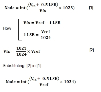
    This present question is targeted to the engineering team at TI. In recent years I have discussed the matter with several experts in industry and book authors. TI seems to be the only company that shows 2^n-1 factor on ADC conversion equation (where "n" is the ADC resolution). In the past, the subject has been discussed a few times, but I think that TI could answer it once and for all.

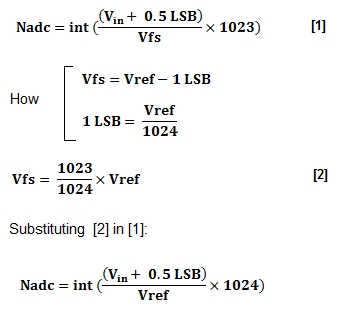
    For example, consider an ideal 3 bit ADC transfer function (figure below): The vertical axis shows seven intervals (2^n-1) and horizontal axis shows eight intervals (2^n). This is true also for 0.5 LSB input compensated ADC. The final transition (from 110 to 111) occurs when input reaches 1 LSB below Vref or 1.5 LSB below Vref. In other words, the transfer functions are something like:

1. For an ideal 3 bit ADC with no compensation on input:

Nadc = int (Vin/Vref*8)

2. For an ideal 3 bit ADC with 0.5 LSB compensation on input:

Nadc = int ((Vin + 0.5 LSB)/Vref*8)

     So, with n = 10, the discussion moves to 1023 and 1024 factors.  The point is that virtually all the other microcontrollers (Renesas, Atmel, NXP, Freescale, ...) exhibit the 2^n factor on equation conversion (than 2^n-1) on its embedded ADCs. I think it would be very interesting to see a conversion plot, similar that below, for TI microcontrollers (ex. MSP430);  but no one can find it.

  • Did you count the number of different values in your drawings? You can't express both, 0 and Vref if your step size is 1/(2^n). So if 1LSB has the value of (1/8)VRef, you have 9 different values from 0 to VRef.

    Those ADCs with a Vref*1/(2^n) step size can't give Vref as result. It is not a matter of compensated input or not.

    IMHO, it is better to have both, 0V and VRef in the output rage than to have the (already rounded this or that way to 1 LSB) values adjusted on voltage levels that are a 1/(2^n) fraction of the reference.

    (ntoe that I'm not a TI engineer, just a pragmatically rather than dogmatically thinking engineer)

  •    Not so fast. You have replaced my words ("interval" by "value"). Please, read my post carefully. As I said, this is not a newbie question. TI needs to answer:

    "Where' s the  ADC transfer function plot (for MSP430, TMS,...)"

  • Rodrigues said:
    Not so fast. You have replaced my words ("interval" by "value"). Please, read my post carefully.

    I did, and it was intentional. The result of an A/D conversion is a value that corresponts to a voltage value (or a voltage interval, but mos tpeole want a voltage, not a range of voltages as result, so they don't think of it as intervals, but ratehr as values with error.). If you have 8 output values (3 bit), you can name 8 input values or 8 input intervals. If you divide the reference voltage by 7 instead of 8, you have grater steps between values (or larger intervals), but you can include both, 0 and Vref into the output range. If you divide by 8, you cannot include VRef into the range of output values, or the highest value has a different error (or spans a different interval size) than the others. Which won't be different from not inlcuding VRef into the output range.

    That's what i wanted to express.

    Besides this advantage, it is AFAIK the natural outcome from an SAR ADC with charge distribution method.

  •      Sorry, but your arguments have nothing to do with my question. As I said, I'm waiting for the response of a TI engineer involved with MCU - ADC integration.


  • Rodrigues said:
    Sorry, but your arguments have nothing to do with my question.

    I don't think so. You declared:

    Rodrigues said:
     TI seems to be the only company that shows 2^n-1 factor on ADC conversion equation (where "n" is the ADC resolution).

    JMG answered:

    Jens-Michael Gross said:
    it is AFAIK the natural outcome from an SAR ADC with charge distribution method.

    In case you want to draw plot you requested, you can refer to this document.

  •    Well, it seems that asking to read my post carefully (everything is very well explained there) is not adding much. Ok then, lets start to copy what was written there:

       I have discussed the issue with some industry experts and book authors. None of them reached a convincing explanation. I was even encouraged by a TI employee not directly involved with the problem (I can not reveal the name, but it is a highly respected professional) to post my question in this forum to see if someone from TI would respond appropriately. My primary intention is to get an answer directly from TI - So, excuse me, if I knew other way, I surely would (unless you tell me the right e-mail/phone).

    Ilmars said:
    In case you want to draw plot you requested, you can refer to this document

    No. I don't want to draw the ADC transfer function plot. I hope TI show it to us. I'm sure Ti will not deny this request. 

  • Rodrigues said:
    Well, it seems that asking to read my post carefully (everything is very well explained there) is not adding much.

    Well, it seems that you are not reading as well. TI in msp430 manual says about ADC10:

    The digital output (NADC) is full scale (03FFh) when the input signal is equal to or higher than VR+, and zero when the input signal is equal to or lower than VR-.

    Conversion formula is N_ADC = 1023 * Vin/Vref.

    This is all information needed to draw plot. Simple. And yet you stand in position that TI have to draw it for you. Ridiculous.

  •      There's nothing ridiculous. The matter is much more subtle than you think. You were too elementary when affirmed that I have not read the ADC chapter on MSP4340 User's Manual. The equation you mentioned I already knew since 2000, when I started using this processor.  Just to touch on the subject, there are books (including on the MSP430), presenting this equation conversion with 1024 factor (than 1023), for the 10 bit ADC. If you'd care to do some research before you post your answer, would also have noticed that there are many sites and blogs (with program listings) that use either one or the other.

         The issue goes beyond simply drawing the plot, as you tried to turn it. The question also involves for what reasons (technical / architectural) TI use a different mode. I'd like to hear an explanation from TI. As I said (for the nth time), the most commonly used processors employ 1024 weighting factor. This also facilitates the calculations by allowing to replace a division (where expression is reversed in order to find Vin) by right shifts. Now for MSP4340 would need to divide by 1023, even though this processor does not have an instruction for division (must be done in software). 

         The information on MSP430 ADC are so limited that, for example, the User's Manual not mention whether there is some form of compensation on inputs (in LSBs). I could start a long bench test (involving precision instruments), but I have no time for this. I believe it is responsibility of manufacturer to reveal the details of the component that it is selling. The question refers not only to the MSP430, but also to TMS3xxx. I could not find an ADC transfer function plot for these DSPs as well.

          As I said (for the nth time, too), I'm still waiting for a response from TI. I truly believe that many participants of this forum and the other engineers will benefit from the elucidation. And do not just rely on someone giving shots in the subject.


  • Rodrigues said:
    The question also involves for what reasons (technical / architectural) TI use a different mode

    Because ADCs of TI embedded microcontrollers are based on charge distribution SAR architecture.

    Rodrigues said:
    As I said (for the nth time), the most commonly used processors employ 1024 weighting factor.

    Because other manufacturers use different type of ADC, mostly Resistive_DAC+SAR architecture.

    Rodrigues said:
    I'm still waiting for a response from TI.

    Well, ok. It will be helpful indeed. Meanwhile please specify which sources of information have 1024 factor specified for 10-bit TI SAR charge distribution ADC.

  • I do not agree with the technical  arguments proposed by llmars and Jens (1023 factor on equation conversion for TI ADC's due to charge redistribution method).

    Details on other post below.


  • Meanwhile please specify which sources of information have 1024 factor specified for 10-bit TI SAR charge distribution ADC.

  •     I don't agree with the technical arguments proposed by llmars and Jens. Both sustain that the referred transfer function have a associated 1023 factor, instead of 1024, due solely to the fact (supposed) MSP430 ADC would be based on charge redistribution. 

        I explain: In the document "slyt176.pdf" cited by llmars is stated: "All Texas Instruments TLV- and TLC-series sequential serial analog-to-digital converters perform Successive Approximation based on charge redistribution." 

        But, studying some TLV / TLC converters is possible verify: The value 2^n-1 (4095 or 1023) is not obtained  when the input reaches Vref, but in some lower voltage; contrasting with what was stated by llmars and Jens.

    Page 4 of TLC2551 datasheet (12 bit ADC):  

    Zero-scale code = 000h, Vcode = GND

    Full-scale code = FFFh, Vcode = VREF - 1 LSB

    Page 13 of TLV1549 datasheet (10 bit ADC):

       Notice on this plot, that 1 LSB is 3 mV ( = 3.072/1024). The final transition occurs 1.5 LSB below some suitable Vref. The vertical axis shows 1023 intervals (2^n-1) and horizontal axis shows 1024 intervals (2^n).

       Both examples are consistent with the plot and equation showed on my first post (based on 2^n factor, instead of 2^n-1). On second example, with 0.5 LSB input compensation, we have (note the value 1024):

    Nadc = int((Vin + 0.5 LSB) / Vref * 1024)

    Not convinced? Then, I show: For Vin  = 3.0675 V:    

    Nadc = int((3.0675 + 0.0015) /3.072 * 1024) = 1023   (In accordance with the plot)

     Despite this, you have stated that the weight 1023 is due to a charge redistribution ADC (???????????).

    So, I could even propose to llmars and Jens to submit a MSP430 ADC transfer function plot, to be consistent with the following equation:

    Nadc = int(Vin / Vref * 1023)

    From the beginning I mentioned that this was a question directed to the TI engineering team. Now the reason is evident.

  • Rodrigues said:
     Despite this, you have stated that the weight 1023 is due to a charge redistribution ADC (???????????).

    I have no problem to admit that my kinda negligent assumption appears to be wrong. I just read slyt176.pdf myself and find that it is about 2^n factor, not 2^n-1 as in msp430 ADC specs. So, msp430 ADC specs contradict with TI's own documentation (slyt176.pdf).

    Rodrigues said:
    From the beginning I mentioned that this was a question directed to the TI engineering team. Now the reason is evident.

    At last your arguments are convincing - well done. Hopefully we will hear TI comments soon.

  • llmars

    At last your arguments are convincing - well done. Hopefully we will hear TI comments soon 


       I'm glad you understood my request. I also hope that the company can respond soon. Meanwhile, I anticipate that someone can to find a way to put the 1023 factor on AD conversion equation. For example, replacing the Vref voltage by Vfs (full scale). So, regarding the previous plot, such equation would be:

          Nadc = int ((Vin + 0.5 LSB)/Vfs * 1023)

           In this particular case: Vfs = Vref - 1 LSB

      Just do the math and realize: This transformation does not add anything new, only confuses even more. It's just a different way of presenting the same information.  Also, the MSP430 User’s Manual  says nothing about Vfs, only Vref  (indeed, would be no practical to work with Vfs).

  • Rodrigues said:
    For example, replacing the Vref voltage by Vfs (full scale).

    You can't simply replace those. Please pay attention to msp430 ADC10 description: "The digital output (NADC) is full scale (03FFh) when the input signal is equal to or higher than VR+, and zero when the input signal is equal to or lower than VR-. ". In this case Vfs shall be defined as equal to Vref+1 LSB or even... infinite.

  •    llmars,

        the presented equation refers to  transfer function plot  for TLV1549 and other 10 bit onchip ADCs (but not on MSP430). I also does not replace only Vref by Vfs (full scale), but also the 1024 factor by 1023 one. Both representations are equivalent.

    For those who do not want to do the math:

        Precisely the equation mentioned at the beginning of the discussion, for a 0.5 LSB input compensated ADC. But as I've stated, this transformation does not add anything new to the subject. My intention was only to prevent  a possible incorrect association between 1023 factor (in fact 2^n-1) and common TI ADCs and, by correlation, with the MSP430 itself. The important point is to have a response from TI, specifically to this MCU.

  • The reference to TLV and TLC ADCs was interesting. However, those are standalone ADCs. I don't know (and I don't have the time to dig into the datasheets) whether they have internal calibration, do any offset compensation or such things.

    The MSP ADC does nothing of this. So you cannot compare one to the other. This is why I talked about the natural outcome of a charge distribution SAR.

    However, some sanity check:
    We're talking about an error of <0.1% on full scale (gain error), while the Quantization error is +-0.5LSB absolute (independent of the absolute value) and  while the reference voltage has an much higher error (up to +-6% absolute and +-0.01%/°C). Not to count the influence of any external circuitry (the signal source)

    Also, the calibration values (or your own calibration) take the gain error into account, effectively nullifying the effect. This is why I'm suggesting to use >>10 (and integer math) rather than /1023 (and float) for the calculation. The error is minimal and the speed gain is significant.

    Wasting that much time on this issue might be of academical importance, but is rather pointless for the very most real applications.

  •      The issue of ADC inherent errors be possibly greater than the difference caused by the multiplicative constants (1023 or 1024) does not invalidate my initial question. However: If the ADC errors overwhelm the referred  difference, then TI would have used 1024 (instead of 1023). With the advantage of being similar to the ADCs from other manufacturers, as well as not cause confusion.

    The questions remain:

    TI microcontrollers/DSP: Where's the Transfer Function plot for ADC? 

    Also: What the real reason for MSP430 10 bit ADC conversion equation to use 1023 factor, instead of 1024? Similar question for the 12 bit ADC (4095 or 4096). Finally: What are the compensation schemes on ADC inputs (in LSBs for example) ?

    I believe that many users (including me) are awaiting the response from TI.

  •       After thinking a bit more about the subject, I guess there is a possibility I have already answered a piece of my question without intending. See the figure below, which I presented in a previous post:


          All could to be explained if TI names Vfs (full scale) as its Vref. It would be just a naming issue? Well, this has happened in the past, for example: Regarding SPI, TI uses UCCKPL name instead of CPOL, and its UCCKPH is the inverse of CPHA (gain -1).

          I do not know exactly what happens inside the MSP430 ADC (the path of the signals, gains and so on). Maybe the voltage applied to the Vref pin could  be transformed internally into another Vref ' voltage (with gain), so that:

    Vref ' = 1024/1023 * Vref   (yes, I didn't write wrong)

         In this case, both expressions below could be correct (assuming 0.5 LSB input compensation):

    NADC = int ((Vin + 0.5 LSB) / Vref * 1023)

    NADC = int ((Vin + 0.5 LSB) / Vref ' * 1024)

         For example, with a voltage applied on Vref pin = 2.5 V (to facilitate, not using fixed point):

    NADC = int ((Vin + 0.5 LSB) / 2.5 * 1023)

    NADC = int ((Vin + 0.5 LSB) / 2.50244... * 1024)

    Similar operations could be applied on 12 bit ADC, too.  Although seem a plausible explication (MSP430 ADC transforming internally Vref into Vref ' ), I'm not sure.

    So, I would like immensely to hear what TI has to tell us.

  • Rodrigues said:
    TI uses UCCKPL name instead of CPOL, and its UCCKPH is the inverse of CPHA (gain -1).

    Well, UCCKPL is used because it is the USCI polarity bit, in contrast to the USART polarity bit or the USI polarity bit :) Of course, UCCPOL could have been used. Well, in Germany, we say 'names are sound and smoke.' Or, to quote Hupty Dumpty: "The words I use mean exactly what I intend them to mean. Nothing more and nothing less". If one knows that 'UCCKPL==1' means 'Clock polarity idle high' than it doesn't matter how anyone else calls it. More, one knowns what it actually means and which implications it may have. Like with the LPMx names. If people don't know what these macros really mean, they don't knwo how to handle them properly and are surprised when things aren't as they expect.

    Btw: IIRC it was the polarity that is inverse to the Motorola notation, not the phase.

  •     The issue concerning the SPI naming is not the focus of this discussion. Despite my note to proceed, the important thing here is to have a response from TI on initial question of MSP430 / DSP onchip ADC (considering all my previous posts).

    Waiting...

  • Rodrigues said:
    I believe that many users (including me) are awaiting the response from TI.

    No, probably just you. :-)

    Rodrigues said:
    Waiting...

    In all seriousness, I would anticipate that you'll be waiting a long time. Despite what your well-respected TI contact told you, the E2E forums are not a good place to expect to get information from TI employees. Hence the E2E (Engineer To Engineer) in the domain address in your browser.

    People like llmars, JMG, and others, while not TI employees, generally do well in answering others' questions.

    IMHO, you should pursue this through your local TI FAE to put you in contact with the appropriate TI engineer.

  •     Look what you wrote. Is there some technical content? Any contribution? No.

    Brian Boorman said:
    ... I would anticipate that you'll be waiting a long time...

        Do you have a crystal ball? You get anything when trying to prevent TI from answering me.

    Brian Boorman said:
    No, probably just you. :-)

        If someone is not interested in the issue, probably does not even account for its existence (including you). Instead of getting angry, you would make a more useful work trying to answer it. For example, the MSP430 ADC is one few not showing its transfer function in the Manual (look on question title). Don't you think that's relevant? I would like to see you contributing technically with the subject. But...

    Brian Boorman said:
    IMHO, you should pursue this through your local TI FAE to put you in contact with the appropriate TI engineer

    I don't think so. The question is about Silicon Engineering, not Field Engineering.

    I don't care. If TI does not respond (which has no cost), I did my job.
    The open question always will be here...

  • Rodrigues said:

    IMHO, you should pursue this through your local TI FAE to put you in contact with the appropriate TI engineer

    I don't think so. The question is about Silicon Engineering, not Field Engineering.

    [/quote]

    My point was that if you really desire the information you ask about, then, in my opinion, you should have your local FAE find out the name of the appropriate TI engineer in the design group for MSP430. If they are unwilling to help you with that, then in my opinion, they are not doing their job. This is the route that I use when I need to get into the "inside" of TI (or any other mfr). Sometimes it works, other times it doesn't.

    Rodrigues said:
    I would like to see you contributing technically

    I was simply trying to suggest an alternate avenue that you could pursue. That was me trying to contribute, rather than argue a point already argued. (And you made it QUITE CLEAR that you didn't want a technical answer unless it came from a TI engineer!) If you went the route I suggested, and got your answer, then you could always come back here and post a followup for the rest of the world to see.

  • Hello Rodrigues,

    Do you have a particular MSP430 in mind that you are asking about?

    I see your really concerned with conversion factors for the ADC. Is there a particular performance measure you are trying to meet for your application? If you are uncomfortable discussing your application on this forum, could you send a private message to me so we can discuss it offline?

    The reason for the questions is that TI has  a few different ADC modules throughout the MSP430 product line and by understanding what you are trying to do, I can provide more relevant information to you.

    As far as ADCs on TI's DSP products, I cannot comment on them for I am unfamiliar with what ADC type and module they use.  Also in reference to the TLV1549 and TLV2551 product information, although informative of those particular ADC operations, those devices are a separate product line from TI and are not necessarily decisive on how the MSP430 ADC performs or operates.

    Regards,

    JaceH

  • Hello Jace H,

       I appreciate your initiative. It was precisely this kind of help that I expected. Now we can start talking about the issue with TI.

    Just adding: The question refers to the 10 bit and 12 bit ADC SAR cores present on several MSP430 families.

       I'll send you private messages. Only then I will put the results here (to community) and declare the questions as answered.

    Thank you so much.

    Dirceu Rodrigues Jr.

  • Jace H said:
    If you are uncomfortable discussing your application on this forum, could you send a private message to me so we can discuss it offline?

    I am very comfortable to discuss on this forum questions asked by Rodrigues. Would you be so kind to read whole thread and answer open questions? Thank you.

  • Ilmars said:
    I am very comfortable to discuss on this forum questions asked by Rodrigues. Would you be so kind to read whole thread and answer open questions? Thank you.

    I'm sure he did. However, Rodriguez either doesn't need this information for a specific project or doesn't want to discuss this project in the public, in order to reveal why he's interested in such a detail beyond any normal importance. So Jace has offered to discuss this in private.

    Maybe the outcome is posted here then. Maybe it turns out it makes no difference for this applciaiton whether it is this or that way or ignore the lower 4 bits of the result. (e.g. if the applicaiton uses 10% resistors on the ADC inputs, more than 8 bit conversion result are nonsense and /1023 vs. /1024 for the reference is not worth even wasting a thought)

    In Germany we have a saying about the splinter in someone else's eye while not seeing the bar in the own. Without project details nobody can check.

  • Jens-Michael Gross said:
    and /1023 vs. /1024 for the reference is not worth even wasting a thought

    "Ignorance is bliss" does not apply to engineering. Problem is not in the negligible precision differences but in lack of information (plot) and explanations. Honestly - initially I did not care about subject much because for me "N_ADC = 1023 * Vin/Vref" is good enough. However when I stopped to be ignorant and read TI SAR ADC "operation manual" (slyt176), it appeared to contradict with SAR ADC we have in msp430! So we have ADC which operation actually is not quite well defined and reasons why it differs from other SAR ADC's - unexplained. I don't think this is right. We need proper documentation :)

    Jens-Michael Gross said:
    In Germany we have a saying about the splinter in someone else's eye while not seeing the bar in the own.

    Yes, this is good one :) I happen to know this.

  • Rodrigues said:
    TI seems to be the only company that shows 2^n-1 factor on ADC conversion equation (where "n" is the ADC resolution).

    Jens-Michael Gross said:
    it is AFAIK the natural outcome from an SAR ADC with charge distribution method.

        No Jens. You are wrong.

    Jens-Michael Gross said:
    In Germany we have a saying about the splinter in someone else's eye while not seeing the bar in the own.

        ???????

        Please don't make smug comments as they are not called for when you are right and can come back to bite you when you are wrong - none of us is the fountain of all knowledge (as was once said). One more thing: Learn to write my name correctly. I'm brazilian.

    llmars said:
    "Ignorance is bliss" does not apply to engineering. Problem is not in the negligible precision differences but in lack of information (plot) and explanations. Honestly - initially I did not care about subject much because for me "N_ADC = 1023 * Vin/Vref" is good enough. However when I stopped to be ignorant and read TI SAR ADC "operation manual" (slyt176), it appeared to contradict with SAR ADC we have in msp430! So we have ADC which operation actually is not quite well defined and reasons why it differs from other SAR ADC's - unexplained. I don't think this is right. We need proper documentation :)

         I agree with you. Let's wait, because I’ve not yet obtained the answer from TI.

  • Rodrigues said:
    Let's wait, because I’ve not yet obtained the answer from TI.

    I still maintain that you won't get the information that you're asking for from TI in this forum. But you are certainly free to wait.

  • Rodrigues said:
        No Jens. You are wrong.

    Which you already stated. And still the different behaviour in a dedicated ADC of unknown internals is no proof for this or that at all.

    Rodrigues said:
    Please don't make smug comments as they are not called for when you are right and can come back to bite you when you are wrong

    Apparently you missed the context. Wasting time on a 0.1% error is futile if the design of the surroundings implies an error magnitudes larger. And as long as the surroundings aren't known or specified,nobody can tell whether this discussion (which took already way too much time) makes any sense.

    Rodrigues said:
    Learn to write my name correctly. I'm brazilian.

    I didn't meant to insult you or all Brazilians or whomever. I'm very sory of having a typo in your name. I suggest taking a sip of Baldrian if a typo in your name is such a big thing for you. If I'd complain each time someone spells my name incorrectly, I wouldn't have time to write anything else at all.

  • Jens-Michael Gross said:

    ... Wasting that much time on this issue might be of academical importance, but is rather pointless for the very most real applications
    ... why he's interested in such a detail beyond any normal importance
    ... /1023 vs. /1024 for the reference is not worth even wasting a thought
    .. In Germany we have a saying about the splinter in someone else's eye while not seeing the bar in the own
    ... Wasting time on a 0.1% error is futile
    ... nobody can tell whether this discussion (which took already way too much time) makes any sense

        I really do not understand your position. After failing to contribute successfully (which is quite normal in this case, since only TI could do it), you started trying to disqualify my question - also asking everyone to ignore it. That's unpleasant! In a forum, all questions are valid. So, wait for the company has to tell us. Or maybe you think being more able to answer than TI. Certainly not.

    As was very well stated by llmars:

    llmars said:
    Problem is not in the negligible precision differences but in lack of information (plot) and explanations.

  • Rodrigues said:
    you started trying to disqualify my question - also asking everyone to ignore it.

    No, I was questioning the importance of this detail without knowing the overall conditions.
    If you ask a manager, the project outlines are always "zero cost, unlimited performance, 100% precision". Everybody know that this is impossible. Your questions goes towards the 100% precision part, so the question is (and this is also meant for your own sake, as you are still waiting for an answer that didn't come yet) whether waiting for an answer is worth the time.

    I agree that the documentation doesn't cover every detail. However, where's the border between not enough and too much information? I'd too like to have a complete internal schematics of the MSP, so I can answer every question. But I also know that this will never happen. So I ask myself whether certain information is so important that I need to waste time in getting it. Often enough, the answer is 'no' if a look besides the immediate point of interest is taken. And if the answer is 'no', then there is no point in demanding the information or blaming someone for not providing it.

    To inverse Ilmars' statement: If the difference is negligible, then the lack of information is not a problem at all.
    That the engineers approach in comparison to the scientists approach.

    The question why this is of such an importance to you is still unanswered.

  • All,

    Sorry for the confusion and long wait. Here is the proper calculation for  1LSB = (VREF+ - VREF=)/2^n, and of course the last code will saturate to 2^n-1

    Typically:

    If Vref+ = REF and Vref- =0,

    Code = Vin x *2^n /REF, so for a 12-bit ADC, 1 LSB=REF/2^n.

    Vin=0 => Code=0

    Vin=REF – 1LSB => Code=4095, beyond this code saturates at 4095 (12b unsigned representation).

    The codes are equally spread between 0 and 4095.

    We believe this is not made really clear in our documentation and apologize for the confusion. Attached is a representation of this answer.

    Regards,

    JH

    6114.ideal_transfer_function.pdf

  • JH said:

    Sorry for the confusion and long wait. Here is the proper calculation...

    ... Code = Vin x *2^n /REF

       Hi JH,

        thank you for coIlaborating, but I confess not be fully satisfied with the depth of response, considering the delay. But OK, let me see if I understood right:


    With Vref- = 0, then the expressions

    Nadc = Vin * 1023/Vref+      (for ADC10)   [1]
    Nadc = Vin * 4095/Vref+      (for ADC12)   [2]


    shown on User’s Manual for several MSP430 families over a decade, would be wrong?

    And the correct expressions would be:

    Nadc = Vin * 1024/Vref+      (for ADC10)   [3]
    Nadc = Vin * 4096/Vref+      (for ADC12)   [4]


    Could you confirm this?

                Another evidence for the fact expressions [1] and [2] would be inaccurate, is to note that the transfer function plots you attached are consistent with the 2^n factor, instead of 2^n-1, being also similar those I presented in my first post. The expressions would make more sense mathematically by using the int() function.

                Also: The answer did not include something about the ADC input compensation schemes (in LSBs). The distinctions between Vref and Vfs (full scale) were not considered, as well. Of course, if that were important in clarifying.

    Dirceu Rodrigues Jr.

**Attention** This is a public forum