This thread has been locked.

If you have a related question, please click the "Ask a related question" button in the top right corner. The newly created question will be automatically linked to this question.

SPI Flash Communication Problem

Other Parts Discussed in Thread: MSP430FR5739, MSP430F47186

Hello there,

I've already been trying a week to communicate with a SPI Flash Memory (Spansion S25Fl256S )

I'm using a MSP430FR5739 and trying to establish communication but I''ve never got a single byte in return from the Memory.

I've analyzed the communication using a logic analyzer.

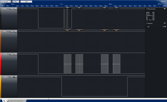
Here's what I've got :

For the time being I'm trying with the Read_ID command.

I Enable the chip, send the clock signal and the command (0x90), then keep on sending the clock signal but there's no returned data from the memory...)

I'm really confused because all the timings, voltage and configuration have been double checked and modified in all ways... but I cannot get it to work untill now ...

Here's my init code for the eUSCB0 SPI Module:

void InitSPI()
{
P1SEL1 |= BIT3 + BIT6 + BIT7; //Select eUSCI Pin Function
P2SEL1 |= BIT2; //Select eUSCI Pin Function
P3DIR |=BIT7;
P3OUT |=BIT7;
UCB0CTLW0 |= UCSWRST; // **Put state machine in reset**
__no_operation();
//UCB0CTLW0 |= UCCKPH + UCCKPL+ UCMSB+ UCMST + UCSYNC; // 4-pin, 8-bit, SPI master
// CKPH = 1 CKPL=1 , MSB
UCB0CTLW0 |= UCMSB+ UCMST + UCSYNC; // 4-pin, 8-bit, SPI master CKPH = 0 CKPL=0 , MSB
UCB0CTLW0 |= UCSSEL__SMCLK; // SMCLK = 4MHz
UCB0BR0 = 0x02; // /2
UCB0BR1 = 0; //
UCB0CTLW0 &= ~UCSWRST; // **Initialize USCI state machine**
__no_operation();
}

Any helpful insight ? Has anyone ever used a Spansion Flash Memory with SPI Communication ?

  • Did you double-check clock and data polarity of SPI flash to match your SPI peripheral settings?

  • Yes, I'm using the Mode 0 with CKPA=0 and the CKPh=0 as well, which is suitable with the device. And the Capture confirms the configuration is correct.

    Thanks anyway...

    Thinking of it I get the feeling that there is something wrong with the powering-up of the Memory because I've never ever received any response from it...  

  • Fredoo.net said:
    Thinking of it I get the feeling that there is something wrong with the powering-up of the Memory because I've never ever received any response from it...  

    Chip Select of flash? Pinout mistake?

  • There was indeed a mistake in pinout where I switched SIMO and SOMI but it has been fixed since.

    Here's my pinout from the flash device, not shown on this is also a 4.7uF decoupling cap on VIO/VCC.

    I've just seen the datasheets mentions a Pull-up resistor on the CS to ensure it isn't selected when powering-up .. ?!?

  • Had to read datasheet and it appears that... well... you did not read it carefully.

    REMS (Read_ID or REMS 90h):  The command is initiated by shifting on SI the instruction code “90h” followed by a 24-bit address of 00000h.

    You are sending FFFFFF instead.

    And please read this: "Manufacturer and device Signature (REMS). READ-ID (REMS) is only supported for backward compatibility and should not be used for new software designs. New software designs should instead make use of the RDID command."

  • Fredoo.net said:
    There was indeed a mistake in pinout where I switched SIMO and SOMI but it has been fixed since.

    If you tend to make such a dangerous mistakes during prototyping, then suggestion is - put series "safety" resistors on every signal line so you don't blow your parts. 470 ohms for 3V running at speeds < 1Mhz shall be fine. If you are in doubt about rise/fall times, check them with scope so they are right.

  • I am using a new PCB with corrected signal routing this time, with a new Memory Chip, so this one should have no reason to be blown up ..

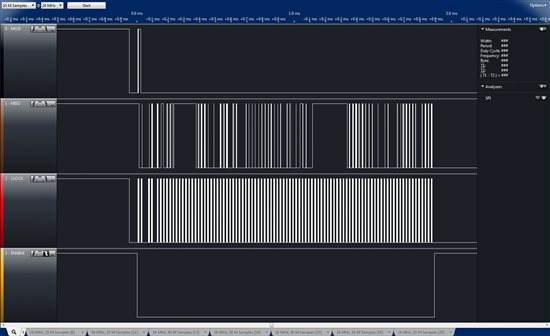
    Also I did see this RDID command which I tried also :

    Here I have the RDID command (0x9F) following by a 24bit 0x000000 address and then the 88bytes of clock pulses... 

    I also just added a Pull-up resistor on the CS with no better results...

    Those safety Resistor you mention are to prevent a too high current to flow from the MCU to the Memory on the output pin ?or should it be put also on the Slave Input pin ?

  • Fredoo.net said:
    Here I have the RDID command (0x9F) following by a 24bit 0x000000 address and then the 88bytes of clock pulses... 

    What about Power-Up? Are you doing it right? Refer to: 6.3.1 Power-On (Cold) Reset

    Also check about CS timing. Or just try to put few clock periods delay between CS and first clock pulse.

    Fredoo.net said:
    Those safety Resistor you mention are to prevent a too high current to flow from the MCU to the Memory on the output pin ?or should it be put also on the Slave Input pin ?

    Those are to prevent high currents when you connect two outputs that may have opposite logic levels. I did not mean any particular line, aspecially for your current design where you are sure about signal connections. Are you?

  • Ilmars said:
    Those are to prevent high currents when you connect two outputs that have opposite logic levels. I did not mean any particular line, aspecially for your current design where you are sure about signal connections. Are you?

    Yes I am sure of my signal connections.. =)

    Ilmars said:
    What about Power-Up? Are you doing it right? Refer to: 6.3.1 Power-On (Cold) Reset

    In my current design I left the RESET pin unconnected and therefore it is mentionned there is an internal Pull-up resistor.

    Therefore I should be fitting in that case :

    And my CS is HIGH due to pull-up ..

    Ilmars said:

    Also check about CS timing. Or just try to put few clock periods delay between CS and first clock pulse.

    Currently there is 4.5uS between the CS Low and first clock pulse (so that's like 5 period for my 1MHz clock signal)

    Thanks for your answers and helpful comments, I'm confident this is gonna work out somehow =) .. just dunno quite how yet ... :$

  • Fredoo.net said:
    In my current design I left the RESET pin unconnected and therefore it is mentionned there is an internal Pull-up resistor. Therefore I should be fitting in that case

    No. You are not. How single pull-up resistor can make delay for reset line? Huh?

    If you are not driving reset pin using uC (you shall), then you shall connect capacitor to it so together they will do tPU delay. I suggest to drive reset using uC according to timing requirements and check results.

  • Hey I got it working !

    I was using the Mode 0 which is CKPA = 0 and CKPH = 0 and therefore I configured 

    UCB0CTLW0 |= UCMSB+ UCMST + UCSYNC ;

    As such...

    But looking in detail there was something wrong with the way the data changed respective to the clock pulses ...

    In the end I used 

    UCB0CTLW0 |= UCMSB+ UCMST + UCSYNC + UCCKPH;

    And got it to respond ...

    Is it due to a wrong reading on my end or is the datasheet misleading ?

    Thanks for your help !

  • Fredoo.net said:
    Is it due to a wrong reading on my end or is the datasheet misleading ?

    I don't know and actually don't want to. You shall find the truth somehow :)

    Don't ignore what I said about reset, do it using uC according to: Figure 6.6 POR followed by Hardware Reset.

    Have a nice electronics!

  • Please refer to S25FL256S data sheet page 79.

    The 90h read id command should be followed by a 24-bit address (000000h or 000001h). Then you will read back the manufacturer id and device id.


  • Hello, my name is Shiu Lee, working for Spansion Engineering Solutions (tech support).  If you have any technical questions related to Spansion products, please visit the following link to contact us for assistance.

    http://www.spansion.com/Support/SES/Pages/Ask-Spansion.aspx


    By the way, S25FL256S data sheet can be downloaded from the following link:

    http://www.spansion.com/Products/Serial-Flash/Pages/Spansion%20FL.aspx


  • Thank you Shiu Lee for coming here, 

    In the end I got it working, I had several trouble that caused me to lose a lot of time mainly :

    • The chip select signal was not always properly coming back up after the end of a command.
    • The configuration of the Mode (Phase and Polarity) were done badly.

    Mostly the problem came from a bad programming/understanding of the microcontroller datasheet, my bad ...

    The datasheet and the documentation of the Spansion chip is quite good, just one thing ... there should be a note in the datasheet software section that wecan download some libraries from the website ...

    I took a good look at theses files : http://www.spansion.com/Support/Pages/DriversSoftware.aspx

    Check the Low Level Driver for SPI Flash

    And it was quite helpful !

    If there is any need I can provide my implementation on MSP430FR5739 for the SPANSION FL-S Device ( I used S25FL256S and S25FL512S)

    Fred

  • Fredoo.net said:
    Is it due to a wrong reading on my end or is the datasheet misleading ?

    Ther eis no generic global SPI standard specification. 'mode 0' is what Motorola calsl 'mode 0'. The TIdocumentation doesn't use these mode numbers anywhere, Instead it calls things as they are: clock polarity idle low or idle high. It is obvious (but inverse to the Motorola notation) that 'CKPL=1' means 'idle high' and 0 means low. Motorola apparently uses 1 for active high and 0 for active low.

    Its always useful to see what bits mean, no matter how they are called and how they are used in different systems.

    So I think it wasn't wrong reading but rather a misinterpretation of what you read based on the wrong assumption of a common notation between different manufacturers. understandeable. And you're not alone - there have been many others fallen into this pit in the past.
    The only reason why I didn't too waste time on the same mistake was my personal preference of knowing what things do rather than how they are named. It takes some time but often saves even more.

  • Fred,

    Thanks for the updates and suggestions. Appreciate it very much.

    Shiu


  • i'm working on a similar project.  i'm connecting MSP430F47186 to the S25FL256S. any place I can find some sample code?

    thanks.


  • You can find very useful code on the manufacturer website :

    http://www.spansion.com/Support/Pages/DriversSoftware.aspx

    Look down for Low Level Driver for SPI Flash

    There is a lof of useful function in the library, you just have to fill in the functions according to your own SPI parameters and with some work it is possible to get through and get it working.

    Regards,

  • please provide your implementation of MSP430FR5739 for the SPANSION FL-S Device S25FL256S.

  • What exactly are you looking for ?

    Spansion provides a very complete generic source code, you can then fill it with your own SPI Read and Write Functions.

  •    Yes sir you are right, i have downloaded that code, Now i am able to read device ID successfully.After that i have called functions-

    1.erase

    2.write

    3.read

    but every time it reads FF.

    i am sending u my code

    1031.sd_card.rar

  • FF is the default value in memory.


    I also had this issue at first.


    When writing data you can only toggle bits from 1 to 0 and this has to be done on what they call a page.


    Then the WHOLE page needs to be erased (every bit to 1 or FF) and only then can it be written to again.

    You have to be careful with the delays between enabling the device and reading the memory.

    Almost  90% of the times I solved reading/writing issues by checking the delays between instructions and such...

  •       Where should i  put the delay please guide me...........

    After CS select or after write enable.

  • In sample program of Spansion they have configured SPI as bellow

    /*
           Set clock frequency to 25 MHz, set 8 DUMMY cycles, disable WP and
           HOLD modes
         */
        WR_R(SPICR, RD_R(SPICR) | SPICR_CLK(0x1) | SPICR_DUMMY(8) | SPICR_WP | SPICR_HOLD);
        
    #ifdef SPI_NAND
        /* Set SPI_NAND_ENABLE bit in the SPI Controller Register */
        WR_R(SPICR, RD_R(SPICR) | SPI_NAND_EN);
    #endif

    #ifdef EXT_MOD
        /* enable extended mode */
        EXT_ENABLE;

    What they mean by "set 8 DUMMY cycles","SPI NAND enable". What should i do in my code.. My SPI configuration is as shown bellow.

     SysCtlPeripheralEnable(SYSCTL_PERIPH_SSI3);
      //
      // SSI 3 configure
      //

      GPIOPinConfigure(GPIO_PQ2_SSI3XDAT0);
      GPIOPinConfigure(GPIO_PF0_SSI3XDAT1);
      GPIOPinConfigure(GPIO_PQ0_SSI3CLK);

      GPIOPinTypeSSI(GPIO_PORTQ_BASE, GPIO_PIN_0);
      GPIOPinTypeSSI(GPIO_PORTQ_BASE, GPIO_PIN_2);
      GPIOPinTypeSSI(GPIO_PORTF_BASE, GPIO_PIN_0);
      GPIOPinTypeGPIOOutput(GPIO_PORTQ_BASE, GPIO_PIN_1);

      SSIConfigSetExpClk(SSI3_BASE, SysCtlClockGet(), SSI_FRF_MOTO_MODE_3,SSI_MODE_MASTER, 1000000, 8);
      SSIEnable(SSI3_BASE);
      GPIOPinWrite(GPIO_PORTQ_BASE, GPIO_PIN_1, GPIO_PIN_1);

  •    oh i got it by adjusting delay.Now i am facing new problem----.

    i have selected n25q256a13esf40f (Flash IC) .Datasheet says that this IC support 54 MHz clock frequency. But when i programed it i found that it support only 1MHz clock frequency.If i increased SPI clock frequency of my controller it does not work.Please tell me what is problem?

    this work for this statement

    SSIConfigSetExpClk(SSI3_BASE, SysCtlClockGet(), SSI_FRF_MOTO_MODE_3,SSI_MODE_MASTER, 1000000, 8);

    but if i increased SPI cloc from 1MHz to 2MHz it does not work.

    SSIConfigSetExpClk(SSI3_BASE, SysCtlClockGet(), SSI_FRF_MOTO_MODE_3,SSI_MODE_MASTER, 2000000, 8);


       Waiting for your response

  • I am sorry to say that I cannot help you any further as I am not using the memory at a high frequency.


    As I remember I am even under 1MHz because I have no use of going higher.

    Maybe you need to send command info at 1MHz and indicate the new SPI Frequency before changing it ?

    So it looks like you are not actually using the Spansion S25FLS and a MSP430FR5739 ?

  •  what is the erase time required to full erase S25FLS256 ????????

  • It is long to fully erase the memory, as far as I remember it is about 10-15 seconds it is given somewhere in the specs I think.

  • Hi Fred,


    I wanted to know if you have any code examples for the S25FL216K SPI flash memory chip interfacing with TI MSP430 MCU by the SPI?

    Can you send me your schematic connection between the MPS to the Flash device?

    Tnx. 

    Hezi.nis@8tec.co.il


  • I am having trouble interfacing with this flash memory. I am not getting any responses. Can you please tell me at what spi frequency you make the flash working??? Really thanks in advance.

**Attention** This is a public forum