This thread has been locked.

If you have a related question, please click the "Ask a related question" button in the top right corner. The newly created question will be automatically linked to this question.

MSP430F5438A & ADXL345 - SPI 3 Wire

Hi,

I've saw that some people already faced to interface the MSP430 and the ACC ADXL345.

I'm trying to establish a SPI 3 Wire communication between both devices, I'm able at least to produce the commands, but I do not receive any data from the device. 

I actually verified with the oscilloscope and I realised that CS (Chip Select) is not behaving as desired:

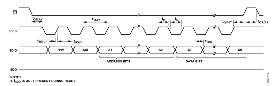
source: Datasheet ADXL345 http://www.analog.com/static/imported-files/data_sheets/ADXL345.pdf , page 16

I saw in the ocsilloscope is not comming in phase, sometimes is delayed. Here it is my code:


void main (void)                                                                                                //Main routine

{

WDTCTL=WDTPW+WDTHOLD;                                                                 // turn off Watchdog

P10SEL|= BIT1 + BIT2 + BIT3;                                                                    // PSEL, SPI for SPI configuration
P10DIR|= BIT0;                                                                                              // CS pin


UCB3CTL1|=UCSWRST;                                                                             // **Put state machine in reset** !!!
UCB3CTL0|=UCSYNC | UCMST | UCMSB | UCCKPL;                         // SPI 3 WIRE, Iddle High, Master Mode, MSB
UCB3CTL1|=UCSSEL_2;                                                                          // Select SMCLK
UCB3BR0=0x02;                                                                                         //Set up SPI CL UCA3BR0 und UCA3BR1, (UCAxBR0 + UCAxBR1 ? 256)
UCB3BR1=0;                                                                                              
UCB3IE|=UCRXIE + UCTXIE;                                                                   // Allow interrupts
UCB3CTL1&=~UCSWRST;                                                                      // Init state machine

while (1)
{

SPI_3_ADXL345();                                                                                    // Call function, write & read

void SPI_3_ADXL345()
{

//Writing some required configuration parameters on the ADXL


P10OUT&=~BIT0;                                                                                   // Set CS as LOW, beginning of transmission
__delay_cycles(2);
while(!(UCB3IFG&UCTXIFG));                                                              
UCB3TXBUF=0x31;                                                                               // Resgister address, 0x31
while(!(UCB3IFG&UCTXIFG));                                                             
UCB3TXBUF=0x4E;                                                                              //Configurate 0x31 with 0x4E
__delay_cycles(2);                                                                               
P10OUT|=BIT0;                                                                                      // Set CS as HIGH, end of transmission

__delay_cycles(10);

//Retriving Device ID ADXL

P10OUT&=~BIT0;                                                                                //Set CS as LOW, beginning of transmission
__delay_cycles(2);                                                                            
while (!(UCB3IFG&UCTXIFG));
UCB3TXBUF=0x80;                                                                            //Retrieve Device ID
while (!(UCB3IFG&UCRXIFG));
Test=UCB3RXBUF;
__delay_cycles(2);                                                                              // Set CS as HIGH, end of transmission
P10OUT|=BIT0;

}

}


I realized that when I'm not transmitting, I don't have clock signal, how can the ADXL send its data to the MSP? ... weird :S


Any suggestion or correction is very well received.


Thanks and regards!

David

  • SPI is give and take. You receive while sending (if there's nothing to receive, you'll still recieve dummy data) and you have to send for receiving (if you don't have something to send, you'll have to send dummy data).

    Actually, the slave cannot know whether the master is sending 0xff or sends nothing and is just clocking for input.
    The 'logic' is in the high-level protocol. If no data is expected, then it is to be discarded.

  • Ok, that explains a lot!

    so now I'm sending dummy data (0xFF), so that gave to me 8 clock periods more, so now it is possible to receive the data that I need,  but how can I catch the INFO of the slave with the oscilloscope, since they are the same wire? Maybe that's a dummy question! 

    And  I lost the cotrol of P10 Bit 0, it appears whenever he wants :(

    Thank you a lot

    Best Regards

    David 

  • Communication from master to slave goes on MOSI pin, slave to master on MISO. You'll need to catch both, and probably the clock and the CS line too.

    But it seems that this dreaded device does both on the same pin, which isn't exacltly SPI. YOu have two choices to implement this non-standard implementation.

    First, you can connect SOMI and SIMO pin directly. In your software, you must ensure that the byte was sent, then you turn the MOSI pin to GPIO input and send the dummy (which won't leave the MSP then).
    This is the cleanest way, bu tit has some drawbacks: first, you won't reach maximum throughput as you cannot use the double-buffering of the USCI hardware. Also, you'll have to do a busy-waiting for the UCBUSY bit to become low, before you can switch the MOSI pin between USCI and GPIO, which wastes CPU time and makes the code more complex.
    The other way is to put a pullup resistor on the SDIO line and a Schottky diode between the MOSI pin and the SDIO line. This way, if you send a dummy 0xff (or any other '1' bit), the USCI won't drive the bus high (only the pullup will pull it up then), so it won't fight the data coming from the ADXL.
    Drawbacks here are that it isn't exactly low-power anymore, because both, the USCI and the ADXL, will have to fight the pullup, wasting some energy. Also, the pullup limits the maximum bus speed, as it causes a slower rise time than an actively raised signal. But the software then can run as if there were separate data lines for the two directions.

    A scope is mandatory for checking the waveform, but unless you have one with 4 inputs (some digital scopes have additional 'digital' inputs), I suggest also using a logic analyzer. A good and cheap one is the Saleae logic-8 (www.saleae.com). It supports up to 8 digital signals (there's also a 16 bit version), and the excellent PC software (which you can try for free, with a dummy signal generator in demo mode) helps you analyzing known interface formats such as SPI, I2C, UART. Also you can log much longer communications than with a digital scope.

    David Rodriguez said:
    And  I lost the cotrol of P10 Bit 0, it appears whenever he wants

    I don'T see anyhting in the original code that would forfeit control of P10.0.

    What do you mean with 'whenever it wants'? Is it random? Or is ist just where you do nto expect it, but always at the same position of the transfer?

**Attention** This is a public forum