This thread has been locked.
If you have a related question, please click the "Ask a related question" button in the top right corner. The newly created question will be automatically linked to this question.
I'm going to refer to this previous post I started earlier. I am trying to communicate to an SPI master using a MSP430 FR5739, specifically, act like an serial memory device for the SPI master. Right now, I am trying to process an EEPROM read instruction from the SPI Master correctly, but the way I've configured the MSP430 has proven to be too slow. Below is an example of how the SPI processes a EEPROM read instruction.
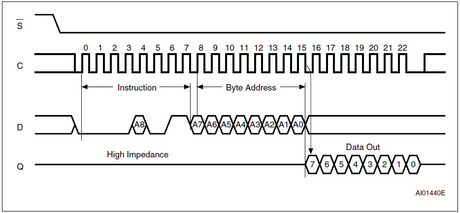
In the picture above, D is the MOSI, and Q is the MISO. The SPI master sends and receives data in sets of three bytes (making 24 clock cycles in total). The first byte is the instruction to the SPI slave (or the MSP430) to read an address from the EEPROM. The second byte is the address it wishes to read from. Then, after the 16th clock cycle, the SPI master will expect to begin reading the contents in the specified address of the EEPROM.
Therefore, what I will need is for the MSP430 to respond quick enough so that between the 15th and 16th clock cycle, the MSP430 will be able to capture the data in a certain address from the memory, and store it in the transmit buffer for the SPI. I currently have an SPI ISR in place so that it can acquire the data aas quickly as popssible. I am doing this repeatedly, so I think DMA may be useful. Does anyone have any suggestions?
I have a couple of updates. I am attempting to use DMA to transfer the data from the specified address of the FRAM, to the transmit buffer of the SPI. Below is some psudo code for what I have in mind.
What is the SPI clock rate you are trying to work at?dauletle said:Therefore, what I will need is for the MSP430 to respond quick enough so that between the 15th and 16th clock cycle, the MSP430 will be able to capture the data in a certain address from the memory, and store it in the transmit buffer for the SPI.
Trying to do this with a SPI slave in software would require a detailed study of instruction latencies to determine if the data out can be written to the SPI Tx buffer in time.
Chester Gillon said:What is the SPI clock rate you are trying to work at?
Since the MSP430 is acting as an SPI slave, the SPI clock rate is set by the SPI master. The clock rate it is running at is at 250 kHz.
I did try to implement a DMA transfer from the FRAM to the SPI transmit buffer. The code is shown below.
void InitializeDMAForSPI(void)
{
DMA0SZ = 1; // Block size
DMACTL0 = DMA0TSEL__DMAREQ ; // DMAREQ triggered
// DMADT = 0 (Single Transfer),
// DMADSTINCR = 0 (Destination address is unchanged),
// DMASRCINCR = 0 (Source address is unchanged),
// DMADSTBYTE = 1, (Select destination as byte)
// DMASRCBYTE = 1, (Select source as byte)
// DMALEVEL = 1, (Level sensitive, high level selection)
// DMAIE = 0, DMA Interrupt disabled
DMA0CTL = DMASRCBYTE + DMADSTBYTE;// + DMALEVEL;
__data16_write_addr((unsigned short) &DMA0SA,FRAM_START+UCA0RXBUF);
__data16_write_addr((unsigned short) &DMA1DA,(unsigned long) EUSCI_A0_BASE+0x0F); //TXBUF Register
DMA0CTL |= DMAEN; // Enable DMA0
}
The above is used to set up the DMA for a transfer. The way the DMA is initiated is shown below.
int main(void)
{
SYSTEM_init();
while (1)
{
while (!(UCA0IFG & UCRXIFG));
if ((RXData == 0x03) || (RXData == 0x0B))
{
FRAM_Read = TRUE;
}
}
}
#pragma vector=USCI_A0_VECTOR
__interrupt void USCI_A0_ISR(void)
{
if (FRAM_Read == TRUE)
{
DMA0CTL |= DMAREQ; // Enable DMA0
FRAM_Read = FALSE;
}
else
{
UCA0TXBUF = 0x00;
RXData = Temp_SPI_Read;
}
STROBE1_LOW;
UCA0IFG &= ~UCRXIFG;
__bic_SR_register_on_exit(CPUOFF);// Wake up to setup next TX
}
Below is an image to measure the latency of my program. Keep in mind that D5 is the time that the DMA is trying to access the data in the FRAM and transfer it into the SPI transmit buffer, while D3 is when the SPI interrupt is initiated.
In this oscilloscope reading, it does appear that the transfer to the SPI transmit buffer completes during the first clock pulse of the SPI transfer. From what I can tell, it does look like I have latency issues. I'm not sure if the MSP430 is quick enough to get the FRAM address from the SPI receive buffer, then use it to transfer a byte from the FRAM to the SPI transmit buffer. It needs to do all of this in a short amount of time, and if it is possible, I would like to know
dauletle said:
I know I have been helping you in the other threads relating to this project, but this is the first time I have seen what you are really trying to do. When I look at this picture I have to be honest, I think "no way with MSP430". Which of course is the same as "yes you can do it but you will have to impose significant limitations that a real EEPROM device does not impose." Most significantly you will need a drastic limit on the SCLK rate. And required time between transactions (CS-high to CS-low again). And perhaps other limitations that may negate the original intent of the project (whatever the intent is).
Very tough project! Good luck!
Jeff
If the project allowed emulation of a I2C EEPROM, rather than a SPI EEPROM, then emulation using a MSP430 sounds possible since with I2C the slave can hold off the master until the slave is is ready. But as you say we don't know what the real requirement for the project is.Jeff Tenney said:I think "no way with MSP430". Which of course is the same as "yes you can do it but you will have to impose significant limitations that a real EEPROM device does not impose." Most significantly you will need a drastic limit on the SCLK rate. And required time between transactions (CS-high to CS-low again). And perhaps other limitations that may negate the original intent of the project (whatever they are).
I'll try my best to respond to both of the replies.
Chester Gillon said:But as you say we don't know what the real requirement for the project is.
I can go into further detail if necessary, but in short, I'm trying to emulate a SPI EEPROM. The master unfortunately does not have support for I2C, which, as you've pointed out, gives a little more control to the slave device I am programming. I did also see details on using the I2C module with the DMA controller in the User Guide.
Jeff Tenney said:no way with MSP430
I am a little surprised that it would not be possible with the MSP430. I have seen other 8-bit microcontrollers emulating a SPI EEPROM the same way that I am trying here, and have been close to matching the specs for the MSP430 FRAM series. In fact, one of the reasons why I chose to work with this device was because some of the specs (notably the internal memory write speeds) surpassed most of it's competition. I initially started working with this series of the MSP430 with the idea that the quick write time would be efficient enough to acheive proper emulation, but it's starting to look like the internal clock is causing this latency.
Jeff Tenney said:Most significantly you will need a drastic limit on the SCLK rate.
Interesting, but how would it be possible to impose a limit on the SCLK rate where the SPI master is the one controlling it?
Jeff Tenney said:Very tough project! Good luck!
Thanks. It is surprisingly reassuring to hear from someone else that this project would not be straightforward. I definitely appreciate the speedy, thorough support I've been getting, and this will encourage me to maybe use your chips in future projects.
dauletle said:how would it be possible to impose a limit on the SCLK rate where the SPI master is the one controlling it?
Exactly. You would have to specify it on paper. "The master shall not use a clock exceeding 250kHz." Or something like that.
You would also need something like, "The master shall provide at least 10us between the rising edge on SS and the subsequent falling edge."
The problem is if the master is expecting to communicate with an actual 8-bit EEPROM, it will not already know about these new rules you added.
Having said that, the FR series can probably do the emulation as well as any 8-bit microcontroller out there at 25MHz. So if you have seen it done before and there is a successful application for it, the you can be successful too. You could probably get it working up to 250kHz with dedicated state-machine code, meaning no other functionality when in EEPROM emulation mode. You would not need DMA or even interrupts.
Jeff
Is the only function of the MSP430FR5739 to emulate a SPI EEPROM, or will the MSP430FR5739 have to handle other tasks (which could affect the latency)?dauletle said:I can go into further detail if necessary, but in short, I'm trying to emulate a SPI EEPROM.
If you are just trying to use a FRAM based MSP430FR5739 to emulate a SPI EEPROM to get faster non-volatile memory writes and/or higher endurance, why not use a FRAM SPI memory such as a FM25V10 - 1Mb SPI FRAM - Ramtron?
Replying to both statements:
Jeff Tenney said:meaning no other functionality when in EEPROM emulation mode.
Chester Gillon said:Is the only function of the MSP430FR5739 to emulate a SPI EEPROM
The only function for the MSP430 is to emulate a SPI EEPROM. The only reason why we didn't just get an off-the-shelf memory chip was because the SPI master requires some unique specifications that don't work with other memory chips. The main benefit from using a microcontroller is that any unique request from the SPI master can be programmed onto a microcontroller, and thus the microcontroller can handle it. At this time, there has been no other functionality implemented on the device other than to do the emulation. Below is some example code on how I am trying to respond to a read request from the SPI master.
unsigned short EEPROMread(unsigned short EEaddress)
{
unsigned short *FRAM_read_ptr;
FRAM_read_ptr = (unsigned short *)(FRAM_START+EEaddress);
return *FRAM_read_ptr;
}
void SPI_force_read(void)
{
while (!(UCA0IFG & UCRXIFG));
}
void SPI_write(unsigned char TX_Data)
{
UCA0TXBUF = TX_Data;
__bis_SR_register(LPM0_bits + GIE); // CPU off, enable interrupts
}
int main(void)
{
SYSTEM_init();
while (1)
{
SPI_force_read();
if ((RXData == 0x03) || (RXData == 0x0B))
{
SPI_force_read(); // read the address from the SPI master
TXData = EEPROMread(RXData); // read from eeprom the data on the address fetched
SPI_write(TXData); // send the data read from the EEPROM to the SPI master
}
}
}
#pragma vector=USCI_A0_VECTOR
__interrupt void USCI_A0_ISR(void)
{
Temp_SPI_Read = UCA0RXBUF;
if (Temp_SPI_Read == 0x05)
{
while (!(UCA0IFG&UCTXIFG)); // USCI_A0 TX buffer ready?
UCA0TXBUF = Status_Reg;
}
else
{
UCA0TXBUF = 0x00;
RXData = Temp_SPI_Read;
}
UCA0IFG &= ~UCRXIFG;
__bic_SR_register_on_exit(CPUOFF);// Wake up to setup next TX
}
In my opinion, I'm not sure how else to make it any simpler than what it is now. Any thoughts?
I guess, with 25MHz CPU speed and interrupt handling, you should be able to go as high as 500kHz SPI clock speed.
With hand-crafted ASM code and busy-waiting loops and no interrupts, up to 1.5MHz are imaginable.
If you limit the data size to 256 byte (Not needing the A8 bit for the addressing), perhaps 2,5MHz are possible.
This includes tricks like holding the RXBUF address in a register etc. to save as many CPU cycles as possible.
The limit is that you have to read teh address and write th eindexed data into TSBUF within 1/2 clock cycle.
If you carefully count execution times and exactly knwo the master clock speed, you can spare the checking for the RXIFG bit for the second byte, saving a few more cycles. However, it is very tricky. And you definitely cannot reach the SPI speed you could with a hardcoded state machine or similar.
Even DMA won't help much. You'd have to write the source address to the DMA source address register per DMA, whcih won't work. Also, the triggering woudl be way more compled. And finally, the DMA still requires soem MCLK cycles for the transfers. Doign this in 1/2 SPi clock pulse is not that much easier than doing it with the CPU.
Jens-Michael Gross said:I guess, with 25MHz CPU speed and interrupt handling, you should be able to go as high as 500kHz SPI clock speed.
I got a little bit confused with your first paragraph in the last post. I thought that since the MSP430 is acting as the SPI slave, that I cant alter the SPI clock speed. However, I did some calculations myself and I found the following:
I will have to keep researching, but I'm not sure if the 47 MCLK pulses is enough time for the microcontroller to respond (and since it is having latency, I can assume that my current setup is taking more than 47 MCLK pulses). I am curious of how many clock cycles do each of these steps take with my current approach, and am also curious to see if whether or not DMA may reduce these clock cycles.
Jens-Michael Gross said:Even DMA won't help much. You'd have to write the source address to the DMA source address register per DMA, whcih won't work.
It might be helpful to review what I've tried with DMA. I was trying to change the source address before every transfer, but I don't understand why that wouldn't work. The DMA I tried to implemented was mentioned earlier .
Jens-Michael Gross said:With hand-crafted ASM code
Is it worth it to implement this in assembly code, particularly the DMA transfers?
What we're saying is that there is no point in using DMA since you need CPU intervention to look up the data requested by the master. Plus if the slave has no other responsibilities, you could do something like this:
WAIT_FOR_END
BIT.B #SS_PIN, &P1IN
JEQ WAIT_FOR_END
START MOV.W #BASE_EEPROM_ADDR, R4
<...> ; Reset USCI, wait for SS, receive/decode command byte
<...> ; If read command, jump to GET_READ_ADDR
GET_READ_ADDR
BIT.B #SS_PIN, &P1IN ; ~4 (or ~3 if SS_PIN is BIT0, BIT1, BIT2, or BIT3)
JNE START ; ~2 (edit: I rearranged these instructions for efficiency)
BIT.W #UCRXIFG, &UCA0IFG ; ~3
JEQ GET_READ_ADDR ; ~2 (executed twice in longest-latency case)
ADD.W &UCA0RXBUF, R4 ; ~3
MOV.B @R4, &UCA0TXBUF ; ~4
JMP WAIT_FOR_END
In this code, the read command handler can load TXBUF within 20 cycles of RXIFG being set. As you calculated, you have 47 cycles with a 250kHz SPI clock. You wouldn't necessarily have to use assembly language if supporting 250kHz is sufficient. At this point, DMA and ISRs just slow you down.
Jeff
Looks good. But since I wrote my project in C, would I have to rewrite the whole project in ASM, or can I just try this in a separate assembly file?
I think in your case you should write it in C.
A good function boundary would probably be handling the entire SS assertion. For example, in main() you do the WAIT_FOR_END part and the START part. But when main( ) detects the assertion of SS, call "ConductSpiExchange( )" or something. Then when ConductSpiExchange( ) sees SS negated from any state, it can just "break"-"return", or just "return" from the middle if you do that sort of thing. Potentially main( ) could even use LPM while waiting for SS, but worry about that later.
Within ConductSpiExchange( ), just remember that function calls add overhead. So don't call functions during time-critical operations. ConductSpiExchange( ) should also be state-based like the asm code I posted.
Jeff
Even if the slave cannot influence the master speed, it has of ocurse an upper limit and can define it in the device datasheet. The master is responsible of not overclocking its slaves.dauletle said:I got a little bit confused with your first paragraph in the last post. I thought that since the MSP430 is acting as the SPI slave, that I cant alter the SPI clock speed.
If you write the source address to DMA source register manually, you can as well write the data manually to TXBUF. You gain nothing.dauletle said:I was trying to change the source address before every transfer, but I don't understand why that wouldn't work.
The problem is that you need to read the two command bytes, assemble the source address and provide the first data byte within these 47 clock cycles. DMA is useless. DMA can be use to transfer subsequent databytes once you set it up, but you won't have enough time to set it up, and once you have the address you have 8 SPI clock cycles to write subsequent data bytes to TXBUF, which can be done easily in software without DMA.
not DMA. I wrote some code that does subsequent TXBUF writes with checking of the RXIFG flag for SPI clock up to 0.5*MCLK (16 MCLK cycles). However, the first transfer takes some time to set up. This is the limit for the USCI anyway in slave mode.dauletle said:Is it worth it to implement this in assembly code, particularly the DMA transfers?
The 47 available clock cycles means a MCLK of 24MHz. However, on a MSP430FR5739 when MLCK is above 8MHz FRAM wait-states have to be inserted. There is a FRAM cache to try and compensate for the wait-states inserted on FRAM access.Jens-Michael Gross said:The problem is that you need to read the two command bytes, assemble the source address and provide the first data byte within these 47 clock cycles.
To try and ensure all 47 MLCK cycles are available for useful work, should the code be run from RAM?
Jeff Tenney said:But when main( ) detects the assertion of SS, call "ConductSpiExchange( )" or something. Then when ConductSpiExchange( ) sees SS negated from any state, it can just "break"-"return", or just "return" from the middle if you do that sort of thing.
I was under the impression that I would conduct SPI exchanges in the SPI RX Interrupt. That way, I can exchange data as soon as possible. Plus, I believe my latency issue is occurring between the second and third transmission, where there is no change in the SS pin.
Jeff Tenney said:So don't call functions during time-critical operations.
Would it be faster if I just insert the contents of the function inside the interrupt? I am a bit rusty on reducing the clock cycles in a set of instructions in C, but are there other pointers you may give that can help this cause (e.g. assign variables into registers for access, insert conditional statements at different areas of the ISR)?
Indeed, on FRAM devices (I completely missed that it was an FRAM MSP), it should. While running code at 24MHz from FRAM is faster than running it on 8MHz (not only due to the cache but also sinve register access and ram/stack access cycles are without waitstates) the gain is still less than the expected factor of 3.Chester Gillon said:To try and ensure all 47 MLCK cycles are available for useful work, should the code be run from RAM?
For maximum execution speed, the code should run from ram.
Note than on FLASH based devices, this limitation doesn't apply.
Jens-Michael Gross said:For maximum execution speed, the code should run from ram.
Just out of curiosity, how would I set up my program so that it is being ran on the FRAM? When I look into the Memory Map when I run the debugger, it does indicate that the memory is set on the RAM.
On a better note, I am getting closer to clearing my latency issues. I moved a bit of the program's logic to the SPI Receive ISR. This is the working version below.
#pragma vector=USCI_A0_VECTOR
__interrupt void USCI_A0_ISR(void)
{
Temp_SPI_Read = UCA0RXBUF;
if (Temp_SPI_Read == 0x03)
{
while ((UCA0STATW & UCBUSY) == 0);
while ((UCA0STATW & UCBUSY) == 1);
UCA0TXBUF = EEPROMread(UCA0RXBUF);
STROBE1_LOW;
}
}
In the case above, I simply read from the FRAM as quickly as I can, and store the read data into the data buffer. Even though this is executing before the SPI clock rises up, making it more efficient may help with my next level of logic that isn't working.
For instance, would moving the logic inside the function EEPROMread(UCA0RXBUF); reduce the number of cycles being used?
The logic that I am trying to implement in the ISR is shown below.
else if (Temp_SPI_Read == 0x0C)
{
while ((UCA0STATW & UCBUSY) == 0);
while ((UCA0STATW & UCBUSY) == 1);
Temp_SPI_Read = UCA0RXBUF;
if (Temp_SPI_Read != 0xB8)
{
UCA0TXBUF = EEPROMread(UCA0RXBUF);
}
else
{
if (UpCntr == 0)
{
UCA0TXBUF = 0xD0;
UpCntr += 1;
}
else
{
UCA0TXBUF = Seed;
UpCntr = 0;
}
}
}
In the example above, I am moving different constants into the SPI Transmit buffer under special circumstances. I was thinking of assigning these constants into registers to reduce cycles, but I'm not sure if that would help. This goes back to the first question on whether or not storing the program into FRAM will allow the program to run quicker.
The code will by default end up in FRAM and run from there. The trick is to move it into SRAM.dauletle said:Just out of curiosity, how would I set up my program so that it is being ran on the FRAM?
There are two ways. You can tell the compiler to tell the linker to put it into ram. Then the function will be stored together with the init values of your global variables and copied from FRAM to SRAM at startup and executed there.
The drawback is that it takes up memory in FRAM (for storage) and SRAM. And since it is copied at startup to SREM, it will be open for any accidental overwrite during operation (until next reset). How this is done depends on the compiler. See the compiler documentation for etails (on CSS, there shoudl be a pragma "#pragma ramfunc" or something like that
The other way is to keep the code relocatable (often enough, it already is, as long as it doesn't use any constants that are stored relative to the function), then reserve some ram with malloc and copy it over right when you need it. The tricky thing here is to know the size of the code to move. You know the beginning (the function pointer), but there is no end marker available. You may use the beginning of the next funciton, but this might fail and has to be checked. on the map after the build.
Indeed, using processor registers (or register variables) speeds up things. This includes access to the target location too.dauletle said:I was thinking of assigning these constants into registers to reduce cycles, but I'm not sure if that would help.
In this case, the loop takes one cycle less than using UCRXBUF as source in the MOV.B instruction.
However, this isn't available for the destination, Sometimes, the compiler will already do this kid of optimization, but it isn't to olikely, as it requires (clobers) one more register (whch needs to be saved and restored) and is one word longer.
Also, if you need to write certain constants more than once, moving them into registers saves anothe rcyycle too. Hwoever, some values (0,1,2,4,8,255/-1,65535/-1) can be provided by the constant generator (actually a read access on the status register in other than register mode) and do not need any space or clock cycle.
**Attention** This is a public forum