This thread has been locked.

If you have a related question, please click the "Ask a related question" button in the top right corner. The newly created question will be automatically linked to this question.

MSP430F5528 USB problem when the cable is normal length

Other Parts Discussed in Thread: MSP430F5528, TPD2E001

I have a board design using the MSP430F5528 and USB. I've designed the circuit using the post on this forum which refers to the Guide "Starting a USB Design with MSP430". I've manufactured 4-5 boards, and have tried to read a lot about USB and look at circuits, reference designs etc. But I have the same problem always.

My design only works when the USB cable is really short. I'm using unchanged examples from the newest MSP430 USB library, including serial port, keyboard/mouse and storage device. For normal length USB cables, my windows 7 computer beeps and the installing driver box comes up, but then it says the USB device is unknown. I've only got it working with a really short USB cable, and not always reliably. 

I wonder which things might be wrong. I've also tried powering from a stable source (not USB). 

Some things: 

- The component is self-powered. Supposed to be with a battery. 

- I've got vias in the USB route since the USB connector is on the other side of the board. 

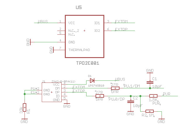
- I'm using 27Ohm R in the USB path and 10pF C to ground on both DM and DP. (Should it be close to the chip or close to the edge)?

- I'm using a TPD2E001, connected to each of the DM/DP on the USB-connector side, with 5V as the VCC. 

- I'm using a diode between the VBUS coming from the USB-connector and my internal VBUS (meaning that the above VCC on the TPD2E001 is slightly lower than the computer's 5V, i.e. 4.9 rather than 5.1V). 

- I've got a 1M from DP to GND and a 1.5K to PUR

I'm really really really struggling. I've been using so long trying to fix this. I would really appreciate any help... 
The board is 4-layered and I'm just showing the top and bottom layers. The other layers are GND (directly below the red top-layer lines) and VCC, below GND. Blue is the bottom. 
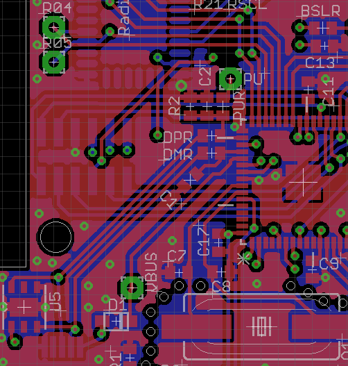
  • Are you sure that PCB D+ and D- traces between U5 and msp430 have right impedance? You have to check not only schematics but also PCB routing guidelines for USB lines. I am not sure that ground trace "antenna" between D+ and D- is right. Hopefully TI engineer can comment in details.

  • Thanks. I would guess you're right and they're not the right impedance. I just don't quite know how to fix it. This would be the 27ohm resistor and the 10pF Cap?

    I've seen that antenna on another design, but I was also wondering whether it was smart or not. I've tried without it (on another design) and had the same problem. I have also tried shorter distance between the chip and the usb port. 

    I found another document now, and it listed a few USB routing guidelines that I seem to have broken. 

    http://www.usb.org/developers/docs/hs_usb_pdg_r1_0.pdf

    - Keep signals in parallel (that's the on you're pointing out also I guess)

    - Put the passive components on the trace, not in a side-line. 

    - Use common mode choke (I don't have one)

    I just wonder how important these routing issues are? Is this likely to be my problem, or is it likely to be something else??? I guess that's hard to answer. 

  • The diode is absolutely on the wrong place, did you try to short it?

    Are the USB components on a ‘clean’ ground, not carrying other digital currents and his noise? Special the 10p capacitors, remove them and try what happens. Also a solid Vcc plane can have (too) high capacitance to the USB traces.

  • Thanks.

    No, have not tried shorting the diode. I'll try. 

    I'll also try removing the 10pFs. Do you think the placement of them and the 27ohm resistors is important, whether it's near the connector or the MSP?

    The layer just below the traces (I hope I've got the ordering right :-) ) is a clean GND (if that means that there are no traces on it at all, just the vias).

    Below that again is the VCC plane. Would it be better not to have the VCC plane under the USB lines?

    Regarding the impedance of the lines. One doc says it should be 90ohms. For a 10 mil trace, would that be 20 mil spacing? Is the thickness of the board, i.e. the distance to the GND layer significant? My current board is 1.2 mm thick and has 4 layers. 

    Sorry for asking what are probably very stupid questions... I've tried to read so much to learn about this, but I find it a bit confusing. 

    Here are some design guidelines I found from an icd.com document. I seem to break some of these. 

    1. Symmetry is the key to successfully deploying differential signals in high speed designs.
    Maintaining the equal and opposite amplitude and timing relationship is the principle
    concept when using differential pairs.
    2. Match the length of each signal of the pair. This ensures that there is no skew between the
    signals of the pair and flight times will be identical.
    3. Route the differential pairs to impedance and at the optimal spacing:
    Gap = 2 x trace width
    4. To control crosstalk – keep aggressors far away from differential pairs especially on
    Microstrip (outer layers).
    A good rule of thumb here is: Gap = 3 x trace width.

  • Digital currents can give a lot of noise. Plains, Vcc or GND, doesn’t guarantee that it’s on the left side of the board is the same as on the right side. If you use these planes on your USB components they will also have that noise. Traces, even very short ones, are inductors and (partly) block the noise, therefore the signals on the USB connector and the USB device are not the same anymore. Try; Wire a separate (off board) USB connector directly as close as possible to your MCU (only tree wires), don’t need, for now, to cut existing connections.

    Did you look with an oscilloscope to the signals?

    By the way, if you try this second connector I would omit the resister and capacitor first, they are not that important, but makes it a little bit difficult.

  • Lars Roland1 said:
    I just wonder how important these routing issues are?

    They are indeed. Usually if you make some exception it will not impact performance much but if you do not follow any of the rules then it can hit you hard.

    You shall put ferrite beads on VBUS and GND (as per document below). Also I see that you don't have ground plane below differential lines but signal traces! This is not good. USB lines are differential so they shall be  without any GND antenna in between. Yes, you are right that resistors and capacitors shall be located close to chip, not in the middle of PCB trace.

    Do you have access to scope having differential probe? Looking at eye pattern will instantly show - your signal is good or you have problems.

    There's TI document you shall read.

    Here's some guidelines and microstrip formulas too:

    http://www.cypress.com/?docID=32407

    Finally I suggest you to check all the reference designs you can find with USB on them, look how traces are routed. Thou I am not sure you will find any 2-layer board with USB ;)

  • Lars Roland1 said:

    I just wonder how important these routing issues are? Is this likely to be my problem, or is it likely to be something else??? I guess that's hard to answer. 

    I have 2 MSP430F5xx USB boards, done by p2p, that I am using for USB based projects development. Both of them are working OK, and never have any problems related to USB (except when firmware was wrong).
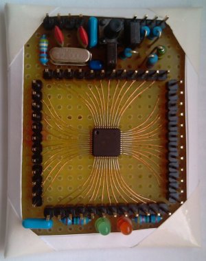
    As you can see, layout is bad, without standard USB connector, but don't have any problems with cable lenghts,  1 MB/s transfer rates, or whatever. Your problem is something else.
    And I don't understand why you are making pcb in only 4 layers, when you can make it in 10, 20 or 50.
    This is your topic here?
    For perfect USB layout (and without crossing DP/DM lines), read this topic...
  • Yes, that first one is mine. Thanks for the second link. I read it earlier, but clearly not well enough. Several points I've missed. Seems very good and I will study it. 

    Thanks for the picture and info on your working board also. 

  • Thanks  Ilmars. That's very good input. I have a lot to fix now :-) and will hook up my scope!!

    There is a ground plane directly below the USB lines, but it's not shown on the picture. Sorry for not making that clear. Will it still be an issue to have the signal lines crossing below that GND plane? 

  • Lars Roland1 said:
    Will it still be an issue to have the signal lines crossing below that GND plane? 

    Definitely not. Perhaps I did miss info that you have 4-layer PCB.

    Before you draw new board - please find what's wrong with particular one. Maybe problem is ground noise and signal lines are just slightly degraded but not main source of the problems. Perhaps you can add ferrite beads using scalpel and soldering iron. If you have scope with diff probes (single ended will not do the job!) and see eye patterns then first thing you do - try to tune RC filter on D+/D- lines.

  • Thanks. I will do. That has probably been my main problem, drawing a new board with some changes and hoping. Without really getting into debugging the existing circuit. I'll take it as learning not just for this board, but also future ones. 

**Attention** This is a public forum