Other Parts Discussed in Thread: CDCE62005, MSP430F5438A
Hello,
I am using the MSP430F5438A uC to configure the CDCE62005 on my board.
When I power up the board the CDCE62005 device loads with the factory defaults and I can measure the clock outputs (e.g output 4 is 125 MHz LVCMOS).
When I try to send a configuration data to any of the device output registers (0-4) the output signal is terminated.
I monitored the SPI bus and it seems like I'm sending the correct data, clock and LE signals (~1MHz clock).
To test the interface I sent only the default values without changing them, just to check if I can configure the device properly to its default values.
My next test was to read the data from one of the registers to see if the data was written properly.
I sent a read command from register 0 and looked at the SPI bus data. The data was correct except for 3 leading zeros before the correct data arrived (don't know if its just 3 extra clock cycles before the valid data arrives).
I tried to read the data from the SPI RX buffer but didn't get the expected values.
What is wrong with my method?
Please see my code below:
#include <msp430.h>

struct spi_data
{
	unsigned char one;
	unsigned char two;
	unsigned char three;
	unsigned char four;
};

struct spi_data MST_Data;
unsigned char RXdata[4] = {0,0,0,0};
unsigned char* pRXdata = RXdata;
unsigned char address;

int i;

int main(void)
{
	WDTCTL = WDTPW+WDTHOLD;                   // Stop watchdog timer

	P1DIR |= 0x40;
	P1OUT &= ~0x40;                            // Set P1.6 for LED


    P3DIR |= 0x80;                            // p3.7 -> SPI LE
    P3OUT |= 0x80;							  //Set LE high

//    P4DIR |= 0x01;
//    P4OUT |= 0x01;

    __delay_cycles(40);


	P5SEL |= 0xC0;                            // select A1 SPI data
	P3SEL |= 0x40;                            // select A1 SPI clock
	UCA1CTL1 |= UCSWRST;                      // **Put state machine in reset**
	UCA1CTL0 |= UCMST+UCSYNC+UCCKPL;          // 3-pin, 8-bit SPI master
                                              // Clock polarity high, LSB
  	UCA1CTL1 |= UCSSEL_2;                     // SMCLK
	UCA1BR0 = 0x02;                           // /2
	UCA1BR1 = 0;                              //
	UCA1MCTL = 0;                             // No modulation
	UCA1CTL1 &= ~UCSWRST;                     // **Initialize USCI state machine**
	UCA1IE |= UCRXIE;                       // Enable USCI_A1 RX interrupt

	//Set SPI data for registers 0-4 (default values)
	for(i=0; i<5; i++ )
	{
		if(i==0)
		{
			address = 0x0;
			MST_Data.one = 0x2 + address;
			MST_Data.two = 0x03;
			MST_Data.three = 0x84;
			MST_Data.four = 0x81;
		}
		else if(i==1)
		{
			address = 0x1;
			MST_Data.one = 0x0 + address;
			MST_Data.two = 0x03;
			MST_Data.three = 0x84;
			MST_Data.four = 0x81;
		}
		else if(i==2)
		{
			address = 0x2;
			MST_Data.one = 0x0 + address;
			MST_Data.two = 0x03;
			MST_Data.three = 0x86;
			MST_Data.four = 0x81;
		}
		else if(i==3)
		{
			address = 0x3;
			MST_Data.one = 0x0 + address;
			MST_Data.two = 0x03;
			MST_Data.three = 0x86;
			MST_Data.four = 0xEB;
		}
		else
		{
			address = 0x4;
			MST_Data.one = 0x1 + address;
			MST_Data.two = 0x03;
			MST_Data.three = 0x86;
			MST_Data.four = 0x01;
		}


		while (!(UCA1IFG&UCTXIFG)); // wait for A1 TX ready

		P3OUT &= ~0x80;				// set LE to low

		__delay_cycles(10);			// wait

		// Transmit data one byte at a time
		UCA1TXBUF = MST_Data.one;
		while (!(UCA1IFG&UCTXIFG));
		UCA1TXBUF = MST_Data.two;
		while (!(UCA1IFG&UCTXIFG));
		UCA1TXBUF = MST_Data.three;
		while (!(UCA1IFG&UCTXIFG));
		UCA1TXBUF = MST_Data.four;

		__delay_cycles(40); // wait

		P3OUT |= 0x80;			// set LE to high

	}

	// set command to read from reg 0 RAM
	MST_Data.one = 0x0E;
	MST_Data.two = 0x0;
	MST_Data.three = 0x0;
	MST_Data.four = 0x0;

	while (!(UCA1IFG & UCTXIFG));               // wait for A1 TX ready
	P3OUT &= ~0x80;								// set LE to low
	__delay_cycles(10);							// wait
	// Transmit command
	UCA1TXBUF = MST_Data.one;
	while (!(UCA1IFG & UCTXIFG));
	UCA1TXBUF = MST_Data.two;
	while (!(UCA1IFG & UCTXIFG));
	UCA1TXBUF = MST_Data.three;
	while (!(UCA1IFG & UCTXIFG));
	UCA1TXBUF = MST_Data.four;
	__delay_cycles(40);

	// set LE for device data transfer
	P3OUT |= 0x80;		// set LE to high
	__delay_cycles(40);
	P3OUT &= ~0x80;     // set LE to low

	__delay_cycles(40); // wait for data
	P3OUT |= 0x80;		// // set LE to high

  __bis_SR_register(LPM4_bits + GIE);         // Enter LPM4, enable interrupts
}

// A1 RX ISR
#pragma vector=USCI_A1_VECTOR
__interrupt void USCI_A1_ISR(void)
{
  switch(__even_in_range(UCA1IV,4))
  {
    case 0: break;                          // Vector 0 - no interrupt
    case 2:                                 // Vector 2 - RXIFG
    while (!(UCA0IFG&UCTXIFG));
	*pRXdata = UCA1RXBUF;					// read RX buffer
	pRXdata++;

      break;
    case 4: break;                          // Vector 4 - TXIFG
    default: break;
  }
}
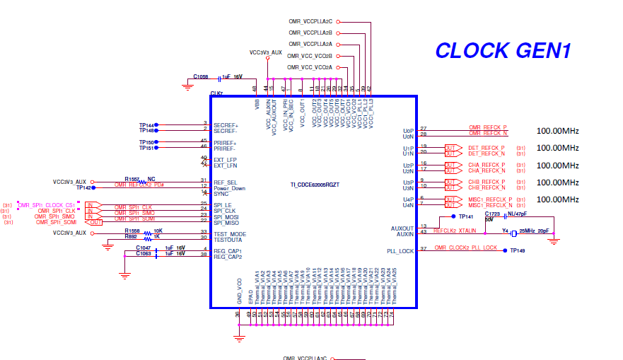
Also see the relevant part of the schematics: