This thread has been locked.

If you have a related question, please click the "Ask a related question" button in the top right corner. The newly created question will be automatically linked to this question.

MSP430F5419 / MSP430F5419A Stability issues.

Other Parts Discussed in Thread: MSP430F5419A, TPS5420, MSP430F47187, MSP430F5438A, MSP430F5418A

Hello there:

Since year 2000 I’m working with many families of MSP430 and I never before faced such problems like now. This is my first project using F5419 and the MCU’s behavior is erratic.

After read the errata sheet, I thought that it could be a general fault on “non A” MCU’s versions. After this, I changed from F5419 to F5419A and the stability is better but not satisfactory.

Basically, the system is a pair of PCB’s where a local unit (using a F5419A) communicates via RS485 with a remote unit (using a F149). The local unit also uses a keyboard, a RS232 GPS, 7 channel ADC, a rs232 serial controller OSD (on screen display), an external RTC, a 8MB external EEPROM… and so, it must handle constantly with all those resources. This system is used for remote control/telemetry. All code was developed in assembler using IAR.

Detected issues:

  • Missing PC during program execution:

The MCU seem to be extremely sensitive to ESD or noise. By example; if I touch the GND plane with a metallic object, CPU hangs because PC jumps anywhere. I added a routine to “catch” a “vacant memory access” event using IRQ’s and adding a breakpoint on that IRQ service routine I noticed that usually, the return address on the stack points to 00000h and rarely to other address far from main code memory. An “ugly” workaround was to generate a “partial reset” of the application jumping from this IRQ routine to the main loop after reinitialize stack and IRQ’s. (really ugly workaround, but it helps to handle about 90% of cases)

This situation is only triggered when I touch a GND plane with a metallic object or when I generate an ESD noise with a fluorescent light. It never happens if I leave the system running for hours or if I use menus or control functions. The ground plane was checked and is consistent, and enough decoupling and filtering is provided for the MCU and peripherals.

From my experience with MSP430, I never before saw such sensibility to noise.


  • Missed or wrong code lines at device programming:

This is really strange because I never before saw something like that. After program a device sometimes it presents a wrong program flow (like if removing code lines).

Specifically; if I press the button to enter in the configuration menu, the system goes inside the menu and jumps out instantly. This happens “always”, no matter how many times I reboot system. But, if I re-program the MCU with the same code, the program flow is normal. (I mean, if I press the button to enter to config menu, system goes inside menu and stay there as it should be)

I have seen this fault about 4 times during the development process, and always in different program parts.


As additional information: previously I was researching about those issues with Mr. Michael Stevens (from TI customer’s services), he checked PCB design and schematics and agreed that all was ok. Reset circuitry, decoupling, filtering, etc… We agreed that after build a second prototype I was going to contact him again to give a follow up. But unfortunately, I was derived to this forum and I have to expose the issue again from the beginning.

So…. any Idea?

Thanks.

Miguel

  • The clamp diodes on the MSP pins, while protecting the device, have the side-effect to route transients from port pins to the supply. This together with maybe sloppy SVS handling may lead to an increased sensitivity for ESD.

    Also, the multiple supply pins and the separate VCore pin require more attention when doing the layout. Short traces between VCore and the cap, distribution of decoupling caps on the different VCCs, all this may matter.
    It depends on actual application (e.g. load currents on different port pins etc.). A logically identical signal (VCC) might be not exchangeable when it comes to physical usage.

    About the missing/wrong code: In release mode, with optimization turned on by default, the compiler will generate different code than in debug more, where optimization is usually off.

    Sometimes, it just seems that code is missing, but it has been moved to where it makes more sense. When debugging optimized code, it may seem you skip code, but in fact the code has already been executed before. When source-stepping, the debugger looks for the current PC in a lookup table to find the location in source code. And if the code has been moved, there is no assembly code at the current point of execution that points to the expected line in the source. And it seems as if the code in this line is not there. But it has been executed before (silently, between two other lines of source code) or wil be execute later.

    This gets worse if you have duplicate code that has been merged. So one PC location could mean multiple locations in source code. Also, sometimes, code indeed gets removes, if it doesn't serve any purpose (from the C language view, which is the compiler reference, no matter what the coder wanted to do, e.g. wasting time)

    Of course there could be other issues too (like insufficient/instable programming voltage during programming, leading to code that 'vanishes' after some time)

  • Jens-Michael Gross said:
    ...

    About the missing/wrong code: In release mode, with optimization turned on by default, the compiler will generate different code than in debug more, where optimization is usually off. ...

    I think you misunderstood this problem (or I am the one that misunderstood). From his description, it sound like the code image was not written correctly (edited by ocy) in Flash in those cases during downloading.

  • Hi Jens, thanks for your answer!

    About clamp diodes… ok, it makes me sense. But the strange scenario of high sensitivity is even when I touch the ground plane. When I was using F5419 (non A version), the MCU was hanging even taking my hand about 4cm near to keypad. I solved that adding a shield to keypad wires. But in all my time working with MSP430, is the first time I had to use something like that.

    Usually, I’m careful with PCB topology design, decoupling and unused pins configuration, then I have never issues with that (well… till now)

    About SVS: at the beginning, I used suggested code to set VCore to maximum level in order to work at high MClk, but later, (thinking that may be the origin of the issue) I have disabled SVS.


    Regarding code issues… I understand that “code optimization” is not a matter here because I’m programming 100% in assembler. I’m right?

    …and, may be, I was not clear enough explaining the issue…

    Ok… when I finish code editing, then I compile and I press debug button to upload code into MCU. After this, MCU may present a “wrong” but “not erratic” behavior… I mean, were the code should go somewhere, instead, code is going to a wrong place, but always the same place… like a undesired jump instruction.

    Then, if I exit debugger and press debug button again (without edit code), the code is uploaded again, but now MCU has the expected and correct behavior.

    The MCU is powered with 3.3v from a REG113-3.3 which can deliver about 400mA (with about 150uF of total decoupling plus small caps for noise near to MCU) and Vcore is set to highest level as I’m working at 16MHz… also I’m not using any kind of low power mode. Then, I see no chance to have low voltage during programming.

    ....BUT!... from your words:  “…leading to code that vanishes after some time”… this makes me sense.

    Some weeks ago, I gave prototype to customer to perform some field test, and about a week later the prototype came to me but death. I powered the systems and it just didn’t boot up. After a visual inspection and voltages check, I decided to re upload code to MCU. (same code previously uploaded). After upload code, the system began working normally. So… it makes me sense that of “vanishing code”.

    Any Idea how can I get deep on this?

    Another question… I could not find in datasheet the correct external decoupling capacitors for VCore. Actually I’m using 1uF ceramic. Is this correct?

    Thanks.

  • Yes, if the code is written completely in assembler, then of course C code optimization is not an issue.

    If you have a stable 3.3V supply, programming shouldn't fail. And flash retention should be as expected.

    The 1µF cap might be a bit much if you change core voltage often (for low-power operations). The datasheet lists 470nF in the recommended operation conditions. And at least 4,7µF near the MSP's VCC pins.

    Is this your only board? A possible explanation could be a hair-crack in a supply trace or a bad soldering point. Good enough to make an electrical connection, but not good for any significant current.
    This could also explain the ESD sensitivity.

    Also, overvoltage might cause flash cells to lose content. (had this happen on some 4V PICs in our RF smoke detectors, where the regulator failed and the 9V battery voltage was applied unregulated -  the PICs survived, but the flash content was gone).

  • Miguel Prado Graf said:
    ....BUT!... from your words:  “…leading to code that vanishes after some time”… this makes me sense.

    Does your code contains any flash manipulations, especially erase?

  • Hi Miguel,

    Miguel Prado Graf said:
    Another question… I could not find in datasheet the correct external decoupling capacitors for VCore. Actually I’m using 1uF ceramic. Is this correct?

    It is very important to use the correct cap value on Vcore or you can definitely have erratic operation as you have seen. We cannot guarantee good device operation with a different value than the 470nF specified in the datasheet, as this cap is part of the internal LDO and supply system for the whole part, and it is tuned for this 470nF value. This is what you should use for stable operation.

    In the MSP430F5419A datasheet www.ti.com/lit/gpn/msp430f5419a on p. 40 under Recommended Operating Conditions you will find the 470nF spec for CVcore. In addition, there is another requirement in the same table that specifies the ratio of CVcc to CVcore: CVcc (decoupling caps on DVcc) must be at least 10 times the value of CVcore.

    I would strongly recommend changing the Vcore and decoupling cap values to match the datasheet recommendation before investigating further - this could definitely be a cause of instability in the system, because it may make the Vcore voltage supplying all the digital logic in the part have some instability.

    Regards,

    Katie

  • Katie,

    I was very puzzled by the problem Miguel faced. Thank you for pointing out the importance of Vcore bypass capacitor. You only emphasized the value have to be 470nF. I wonder if low ESC and RFI/EMI suppression are important factors too. That is, do you mean any kind of 470pF capacitor will do the job?

    Regards,

    -- OCY

  • Katie, Jens, IImars… thank you by your comments and support!

    Answering questions (in order):

    Jens:

    There are two identical boards; …a first prototype, were I started using a F5419 and later I changed to a F5419A, and a second equal board since the beginning with F5419A.

    Both of them have the same erratic behavior, then (I think) we may discard the chance of PCB fault. BUT… I noticed that in the first prototype, after replace “non-A” MCU by “A” version MCU, the stability was better.

    I think that “voltage issues” are not very possible because the MCU and analog are powered by a REG113-3.3 which is rough enough… and this one is powered from a regulated 5v switching power supply (TPS5420). After monitoring 5v and 3.3v, I cannot see noise or glitches. (and moreover, I’m using almost same power scheme since long time ago).

    Regarding Vcore, I want to add that I’m NOT using low power operation modes, nor changing Vcore during operation. During MCU startup and config, I set full power and full speed and this configuration is never changed.


    IImars:

    The code does NOT have flash manipulations during normal system usage. Although, there is an access for erasing and writing “information memory” only at the moment of leaving configuration menu, when a new configuration data (parameters) are saved to “information memory”.

    In fact, in “one” of the times that system was performing unstable or hanging, was exactly in the moment of leave config menu (when the new parameters are being written to info memory). The PC was jumping out of main code area triggering vacant memory access IRQ. But I solved that issue re-loading the same code to the MCU, and issue didn’t happen again.


    Katie:

    Thanks for your information. I will work fixing that ASAP to add a follow up about.

    I tried to be exhaustive reading datasheets, but obviously I missed that important detail about Vcore Cap.


    Thanks, and best regards.

    Miguel

  • Miguel


    Katie:

    I just replaced Vcore external Cap by a 470nF. And also I increased near decoupling capacitance from a total of 80uF to about 120uF… But I see no big changes in behavior. Anyway, it’s too early to make a judgment.

    During last testing hours, the system performs stable and seems to be more resistant to near ESD; but if I touch many times the GND plane with anything metallic (after discharge myself, of course) MCU’s PC jums out of code or MCU just resets.

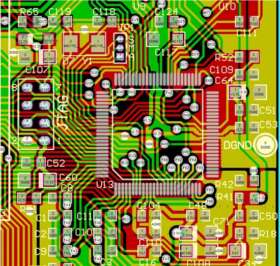
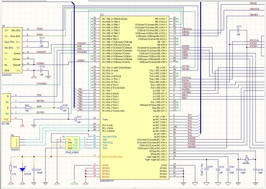
    I’m attaching MCU area PCB layout and MCU schematic. (note: decoupling caps are not snow in schematic. )

    best regards.

    Miguel

  • Miguel Prado Graf said:
    The code does NOT have flash manipulations during normal system usage. Although, there is an access for erasing and writing “information memory” only at the moment of leaving configuration menu

    So your project indeed contains flash manipulation code which possibly could be reason of flash (segment) loss. Besides all circuit-related precautions against crash you are advised to implement crash-safe code. Simple and quite effective solution: do not use FWKEY as constant in your flash manipulation code but as variable of subroutines. Also fill unused code flash with instruction that causes WDT timeout.

  • IImars, thanks for your post.

    I don't think that the access to flash memory could the cause of "code erasing", because after load the code into the MCU the fault may occur even if the flash writing routine was never used.

    Anyway, I would like to try your idea. But I didn't catch exactly how to do it, and, how/why it should have a different effect.

    The only one “info memory” code write routine I’m using is this:

    SAVEINFO	
    	nop
    		
    	//unlock segment
    	mov.w	#FWPW,&FCTL4		;clear LOCKINFO
    	bit.w	#LOCKA,&FCTL3		;mem locked?
    	jz		SVFLSHunlocked	;jump if unlocked.
    								;still locked!
    	mov.w	#FWPW+LOCKA,&FCTL3	;changes lock status
    SVFLSHunlocked				;segment unlocked
    
    		
    	//erases memory:
    SVFLSHbusy0
    	bit.w	#BUSY,&FCTL3		;mem controller busy?
    	jnz		SVFLSHbusy0		;mem controller busy! Jumps to retry
    								;mem controller not busy
    	mov.w	#FWPW,&FCTL3		;release lock
    	mov.w	#FWPW+ERASE,&FCTL1	;enables block erase
    	clr.w	&FLASHSTARR		;dummy-write to erase block
    SVFLSHbusy1
    	bit.w	#BUSY,&FCTL3		;mem controller busy?
    	jnz		SVFLSHbusy1		;mem controller busy! Jumps to retry
    								;mem controller not busy
    
    	//write data block to info memory:
    	mov.w	#FWPW,&FCTL3		;release lock
    	mov.w	#FWPW+WRT,FCTL1	;enables write
    		
    	mov.w	#OSD_BUFFER,R5		;initialize source pointer
    									;NOTE: OSD_BUFFER defined at Even RAM address.
    	mov.w	#FLASHSTARR,R4		;initialize destiny pointer
    									;NOTE: FLASHSTARR defined at info mem start address.
    
    SVFLSHloop	
    	mov.w	@R5+,0(R4)		;copy words from RAM to info mem
    	add.w	#0x0002,R4		;increment destiny pointer.
    	cmp.w	#OSD_BUFFER+56,R5	;compare origin pointer with end of buffer
    	jnz		SVFLSHloop		;jumps if not end of buffer!
    								;end of buffer.
    	//re-lock segment
    	bit.w	#LOCKA,&FCTL3		;mem locked?
    	jnz	SVFLSHlocked			;mem already locked; jumps
    								;mem not yet locked
    	mov.w	#FWPW+LOCKA,&FCTL3	;changes the lock state
    
    SVFLSHlocked					;segment locked
    	mov.w	#FWPW+LOCKINFO,&FCTL4	;clear LOCKINFO
    	call	#DLL500ms			;500ms delay
    	ret
    

    And the code from where it is called is this:

    	//Backup parameters to info mem.
    	call	#DLL100ms			;100ms delay
    	nop
    	dint						;disable interruptions
    	call	#FILL_RAM_PARAM	;build parameters block in RAM
    	nop
    	call	#SAVEINFO			;save data from RAM block to info mem.
    	nop
    	call	#DLL500ms			;500ms delay
    	eint						;re enable interruptions.


    Would be nice if you can give me a hint about how to apply your idea and explain me why it is useful

    Thanks!

  • Hi Miguel,

    Ilmars is suggesting that you could see an erase from the PC jumping to the piece of code where your flash routine is located - especially since you mentioned before that you'd seen the PC jump erratically when you do your testing. This would be a possible cause of seeing an erased area.

    So his suggestion is to calculate FWKEY instead of having it hard-coded as a constant in your code - instead have it be a variable that is calculated over the course of a few instructions mixed throughout your routines that lead up to your flash write.

    e.g. your line

    mov.w	#FWPW+LOCKA,&FCTL3	;changes the lock state

    instead of having #FWPW, which is a hardcoded value, have a variable/register that slowly assembles the correct FWKEY value over the course of the code leading up to the instruction. The idea is so that your PC couldn't just jump to anywhere in your Flash code and cause an erase, it would have to jump to the right place before all of your calculation of FWPW, for the code to actually use the correct FWPW. The rest of the time no flash operation would take place because a wrong FWPW would be use so the operation would be rejected.

    This is a good practice to do, but we should probably try to look further into your instability. Is there any point in your software that you modify the PMM or SVS register settings, or is everything left strictly at default at all times? The reason I ask is that I know there are a number of errata on the F5419A related to the PMM and SVS subsystem: www.ti.com/lit/pdf/slaz282 Please make sure that you have applied the workarounds for all PMM errata that apply to your situation and revisions of the device that you may be using.

    In addition, the PMM and SVS are pretty complex and settings have to be changed in just the right order to avoid problems (as you can see from the lengthy descriptions in the user's guide). For this reason, I strongly recommend that you use driverlib to do any PMM/SVS setting reconfiguration rather than trying to write the code from scratch - the driverlib routines will make sure everything is done in just the right order and that an illegal configuration is not used. I do this even if I'm not using driverlib anywhere else in my project - it is just best practice for this module to avoid mistakes. Now, it looks like you are using assembly mostly which makes this harder (I actually do not see many people program our 5xx devices in assembly), but you could still do this in a mixed C + Assembly project and just use C + driverlib for the PMM/SVS setup. Or you could carefully make your own assembly version of the driverlib PMM configuration function that you would use, using the driverlib function as a guide for what sequence to do each instruction. You should take special note of the sequence for modifying Vcore - the Vcore can only be raised or lowered a single step at a time, and the driverlib code shows this (and how SVS is managed while changing Vcore levels).

    Regards,

    Katie

  • Katie, thanks for your hints.

    About IImar’s idea: ok, I got it! …It makes me specially sense, having in mind that my PC is jumping anywhere!


    Regarding configuration of SVS and PMM, the only point where those registers are modified is at the MCU statup and configuration, after that those registers are not modified again. For setting up those registers, I have used TI’s suggested assembler routines to set them properly.

    Although, I have disabled SVS and associated interrupts, then I think that PMM issues should not be a point here. Also, most of the PMM errata issues make reference to the use of low power modes and issues at wakeup… but this is not my case as I’m not using low power modes. Always system is running at full power and full speed (16MHz).

    ….BUT! …the errata PMM17 may give a little hope… it mentions a maximum limit of 2.0v for Vcore…

    …so… may be, there is an over voltage on Vcore generated by an ESD the reason of missing PC?

    I just performed some tests with boards, as today I was working with both equal prototypes together. Both presents same behavior, then again I discard PCB or electrical faults.

    Actually, both prototypes have a F5419A version and I didn’t saw recently any kind of “code vanishing” or “wrong” code execution.

    Let’s remember, that actually I’m forcing the “PC lost” condition, just touching GND plane with a screwdriver many times.

    The test I performed was to force the system to enter in an “error handler routine”, were interrupts are disabled (except Vacant mem access) and an infinite loop is entered doing “nothing”; at this point, I tried to force the “PC lost” condition and I got it as always. From this test, I think, we may agree that there is not a problem with code…


    May be important or necessary to add decoupling capacitances at “each” pair of DVCC-DGND input pins? (Let’s remember that there are 3 pairs of power inputs; …and I didn’t find any special routing reference about that).


    Regards,

    Miguel

  • Hi Miguel,

    So if I'm understanding correctly, using the MSP430F5419A and the new cap values, you've seen some improvement in behavior, and you no longer see segments of flash being erased. However, if you do a test where you are deliberately interfering with the ground plane, you can still see the PC get corrupted.

    This does start to sound more like all you have left to do is to try to improve noise/ESD considerations on your board. A document that provides a lot of tips on robust design for ESD is www.ti.com/lit/pdf/slaa530 - MSP430 System-Level ESD Considerations. It covers a variety of things you can do to make a robust design.

    Regards,

    Katie

  • Perhaps it has nothing to do with ESD. Touching the GND plane with something metallic means adding your body capacitance to the system. You may pull GND "somewhere" while it takes some time to the change propagate through the system. This may cause temporarily raised or lowered voltage levels.

    This is very difficult to track down, as a scope is usually grounded and may not see this effect or simply nullifies it by connecting the system GND to earth. You'd need an isolated differential voltage sensor to detect this kind of effect.

    As every audio enthusiast can tell you: GND isn't GND, even if directly connected ("ground loop"). And even less if you make and break capacitive connections.

  • Hi Katie and Jens,

    Katie, you got it right about ESD and Flash issues.

    Even still is early to be 100% sure, it seem that I’m not experimenting flash erasing issues.

    But regarding ESD… as Jens said: it has nothing to do with ESD.

    I have read the reference, and it seems that my design is between the boundaries of that reference. But still it is strange… following those design rules and a “electric common sense” I never before had such problems with previous versions of MSP430 (including designs with F122,F133,F149,F169,F4794,F47187, etc...)

    Just minutes ago, I took and plugged an old training PCB I made for myself with a MSP430F47187. It’s a basic PCB WITHOUT any ESD consideration; it has only MCU, crystal+caps, and a pair of decoupling capacitors and the reset network. On this PCB, several tracks are being used to drive a parallel color LCD and remaining tracks reachs unconnected heather's (perfect antennas). This PCB has a simple software that draw and moves a figure on the LCD.

    I placed this PCB based on F47187 together the system based on F5419A (which is the matter of this post) and it works perfectly while F5419A hangs. I have even joined GND’s and touching the GND plane of board with F47187 makes the F5419A to hang, but F47187 continues working without problems.

    Would be interesting to know from other people working with MSP430F5xxxx, if they have seen some unstable behavior due to ESD. I refuse to think that this is happening just to me.

    I really liked characteristics and resources of F5419, but I’m afraid to use it again in a new design.

    Regards.

    Miguel.

  • Only 5xy family uses a core voltage regulator. Also, on the non-A, core voltage was on high level by default, while on the A versions, it is on lowest level.

    Anything that might affect VCore could cause a stability problem. Especially if VCore is on lowest setting.

    Probably, on your board design, any 5x family device would show the same problem, with the 54xx non-A less sensitive due to it higher default.

    What if the first thing you do in your code is raising PMMCOREV to 2 or 3? Does this improve stability?

    Another thing: on which clock speed is your application running? And from which source (DCO, crystal?) To avoid MCLK glitches, you can use a twice as fast clock and use MCLK with a /2 divider. (for a test, just use a /2 divider with your current clock settings and see whether it makes a difference)

  • Hi Jens!

    As described above, the Vcore is set to its highest level at the MCU initialization, and is never modified after this. (the procedure used to set Vcore is the suggested procedure from datasheets).

    In A version and non-A version, behavior was almost the same: high sensitivity to ESD.

    …BUT, I could say that with A version, the behavior is “LESS sensitive”… non-A version was a chaos.


    Regarding suggested things to do… I’m already running at highest Vcore because MCU is running at high speed.

    About the clock source, MCU is running from XT2 @ 16MHz… and as the maximum is 25MHz… it seems complicated to apply 32MHz  and then divide it by 2.  (I need those 16MHz).


    mmmmm…. May be, a nice attempt to set DCO near to 16MHz and clock CPU from it???  (leaving TX2 clk for communications and timing)  

  • On non-A devices, maximum speed was 18MHz, so you have been closer to the max speed.

    It is possible that your crystal has hiccups on ESD event, causing short CPU cycles. On A version, you have more reserve for the maximum CPU speed than on the non-A, so the critical limit is higher and the system is less sensitive.

    You could try the following: output XT2 to a port pin (MCLK/SMCLK output) and check whether it is stable when the device crashes. You might find an erratic clock pulse that crashes the CPU.

    Also, as you described, you may use XT2 for communication only, and use DCO for MCLK (maybe running the DCO on 32MHz, divided by two). Or use a 32MHz crystal and divide by 2, if you don't already need the MCLK or SMCLK divider.

  • Problem solved!

    Yesterday, I decided to fire a last bullet: As Jens said; I changed MCLK to DCO locked with FLL to XT2.

    …and after this, no more missing PC have happened. The only strange point is that I configured DCO for about 16MHz, and after enable FLL referenced to XT2, DCO output goes to 18MHz… (that was not a real problem, just change some constants used to generate delay routines)

    Trying to re-induce system fails, I was even firing a spark plug 10cm over naked system and no hangs have happened. I think this is proof enough that ESD design was not bad.


    Would be interesting if Katie could escalate this issue to TI’s design area. For me it seems to be a mayor issue.


    As additional information: during MCU configuration routines, I was monitoring MCLK at its dedicated pin on port P11. After power up system, as soon as XT2 becomes stable and is selected as MCLK, the MCLK signal at pin is stable and solid; but as code continues, MCLK seems to fluctuate; being not solid anymore.

    Thanks to every one for suggestions and comments, especially to Katie and Jens.

    Best regards.

    Miguel.

  • So it seems, the problem was (and still is) the crystal. If the FLL configuration isn’t buggy, then the crystal you use as reference isn’t stable. Which has caused the problems you had and still causes the DCO to run off. The FLL tends to have some jitter when the reference frequency is near the target frequency, you should use a reference input divider and a higher FLL factor instead of using a 1:1. This would also average any crystal hiccups. However, I’d further investigate why your crystal apparently isn’t stable, now that the clock source has been identified as the weak spot.

    It might be that your capacitors or the PCB layout isn’t good and oscillation amplitude is low. Since the oscillator part is analogue, there is a margin where it may still work on one MSP but not on the other, even though outside the defined or expected parameters for both.

  • Hi Jens!

    I didn’t try to replace crystal, but I will try it ASAP. But still it’s strange, that debugging step-by-step the startup process, after select MCLK from crystal, the output of MCLK looks prefect and stable… but after MCU continues configuration of peripherals, that signal becomes unstable.

    Whatever, from two prototypes, I’m still having serious troubles about “code vanishing” with one of those equipment’s, even both prototypes are not hanging or missing PC. There are no hardware or code differences from one prototype to another.

    I have implemented the protection for Flash writing described in a previous post (…by the way, why Katie’s posts have been deleted???)

    This protection assembles flash password through many steps (not hardcoded) and before each write, it checks the range where pointer is pointing.

    But, the problem is that the RESET vector is being changed; the fault was: system was working stable and without problems, after many power cycles (off-on) in one power up, MCU didn’t boot at all, even cycling power again.

    After connect debugger and get on sync “without re-download code”, I have noticed that MCU was starting from a wrong address… setting reset address manually with debugger (using “set next statement”) and running program from that point, system began running normally. But after a new manual reset, MCU went again to a wrong starting address.

    Accessing flash content window in debugger (not disassembly window), I could see that the reset vector was 0x5000, and the programmed vector was 0x5C00 (code start address and reset address)

    After download the code again to MCU, the reset vector was again 0x5C00 as it should be. But after some power cycles (not writing to flash), again reset vector have changed to 0x5000, so MCU could not boot.

    From this situation, I cannot guess what is the reason why for that fault, and why in one MCU yes and in other no. I’m not using low power configuration or low power modes… a solid power source is used with enough decoupling… flash writing is performed using internal timing generator…

    So? …what else may be origin of this fault?

    At the moment, the only way I can see to catch the moment when this vector is changed, is to write a code trap to check the content of reset vector and freeze the MCU on that moment… at least, to know when it happens.


    Best regards.

    Miguel.

  • This is indeed really weird.
    The reset vector shouldn’t change.
    I could imagine a bug in the flash write code (or the code that calls it), causing a bogus write to 0xFFFE due to an index out-of-bounds problem.
    Also keep in mind that in the MSP instruction set, the fixed part of the indexed address mode is a signed(!) offset and the register is the ‘base address’ part - even though the compiler will use the fixed part as base and the register part as offset. Under some circumstances, this may cause trouble.

    But then I’d expect this to happen on every MSP, not just on one. You could set a breakpoint on access onto the reset vector, so the breakpoint is hit when the vector is accessed (which shouldn’t ever happen while the app is running). Maybe you can then trace back what happened. Keep in mind that during a flash write, any  read access to flash (even by debugger) results in 0x3fff.
  • Hi Miguel,

    Miguel Prado Graf said:
    I have implemented the protection for Flash writing described in a previous post (…by the way, why Katie’s posts have been deleted???)

    I don't think any of my posts have been deleted - however this thread has gotten long enough that it's now on multiple pages so you won't be able to just scroll up and see my posts - you'll need to go to the link for page 1 at the bottom of the page.

    For your latest issue: are both of your prototypes using the MSP430F5419A device (not the non-A version)?

    The fact that it only fails on some parts and not others makes it sound like something marginal is going on (something timing related, or something taking part out of spec where some parts will tolerate it better than others simply due to normal device variation).

    A couple of shots in the dark from my experience with other customers:

    1. You mention that you use the recommended Vcore setup code for setting Vcore to the higher level - is this coming from our core libraries (just wondering if I could see your code)? Or maybe you based your code off of the SetVcoreUp function described in the user's guide www.ti.com/lit/pdf/slau208 on p. 108?

    a. In addition to using this vcore code method, did you make sure to only step the Vcore up only a single level at a time? You have to run the function mentioned in the user's guide multiple times if you want to go to level 2 or level 3, increasing only a single level each time you go through the whole function - I've seen people do all the right steps for waiting til the new level is reached and everything in the right order, but miss this part before and be setting it straight to their desired level instead of doing the whole process multiple times with a single step up each time. If you go straight to level 2 or level 3 at startup, even following the rest of the method from the user's guide, I've seen this definitely cause strange behavior and the behavior will show up more on some parts than others (some tolerate the out-of-spec setup better than others). Just something to double check.

    2. You mentioned in part of the thread that you disable the SVS completely at some point after startup. I would strongly recommend against doing this. Here is the problem - if you disable the SVS, it won't catch if your voltage has a glitch (or at power down when you turn power off). When you are running at 16MHz, you need to maintain a certain core voltage to run properly at this speed - for 16MHz this is Vcore level 2 or 3. To maintain this Vcore level, you also need to maintain a certain Vcc level - in the datasheet Recommended Operating conditions section, you can see that for PMMCOREVx = 3, the min Vcc is 2.4V and for PMMCOREVx = 2 the min Vcc is 2.2V. When your Vcc drops below this threshold for some reason, you are in what we would call a voltage vs. MCLK violation. This kind of violation can cause the part to execute and behave erratically, and perhaps is somehow changing some of the flash of your part (e.g., writing something over your RST vector location). Since you have no SVS enabled, your part will continue to try to run even once Vcc has dropped below this threshold, all the way down to the BOR threshold, and so can be doing erratic operation that whole time as your Vcc drops. Ideally what you should do is set your SVS to be enabled and set to a level that ensures it will catch and hold the part in reset when your Vcore or Vcc drops below an acceptable level for your 16MHz system frequency. If you are seeing your issue occur only after doing tests where you are power cycling the part, I'd definitely consider this a potential culprit. If you leave the SVS enabled with it set to an appropriate level to prevent any voltage vs. MCLK violations for the 16MHz you are running at, does your issue go away?

    Regards,

    Katie

  • Jens, Katie:

    Yes, it is indeed really weird.

    …and specially, having in account that actually I have swapped prototypes and no one is presenting faults; I mean: first prototype (Pt1) which was inside the final equipment and which was faulty, now is in the lab, and the second prototype (Pt2) which was in the lab, is now working inside the final equipment. Both are working without problems till now (after about 5 days of tests). Both have the F5419A MCU and both have same code.

    It’s strange that when the equipment came to my lab to perform the PCB swap, the system (Pt1) was not booting at all, and after connect and get on sync with JTAG (without download code), I could see that reset vector was wrong. After this, I have downloaded the code again and system began working normally, but after two power cycles, reset vector was corrupted again and the system stopped booting again. After this, I took this Pt1 out of the final equipment and I placed Pt2 instead, which began working without problems till now.

    The weird part is that, after take Pt1 apart from final equipment, and re-download code to it, also didn’t fail again on my lab. I have tried to apply heat with a hair drier, to cold down having PCB inside freezer for a while, and no faults again. I have feed the system with a very low voltage to see if the supply was the fault… and nothing happens.

    At this point I didn’t try to return over crystal driven MCLK testing with another crystal (thinking in the previous trouble about missing PC), because at the moment that trouble is overcome using DCO as MCLK. By now,  would like to find the reason of the reset vector being corrupted.

    Jens: Regarding flash write routine, actually is this:

    SAVEFLASH    nop
                 //unlock segment
                 add.w  R5,R4               ;flash password key in R5 (and R4=0)
                 mov.w  R4,&FCTL4           ;clear LOCKINFO
                 bit.w  #LOCKA,&FCTL3       ;mem locked?
                 jz     SVFLSHunlocked      ;jump if mem unlocked
                                            ;mem still locked
                 add.w  #LOCKA,R4           ;adds bit LOCKA to key in R4
                 mov.w  R4,&FCTL3           ;writes “1” to change control state.
    SVFLSHunlocked                          ;segment unlocked
                 //erases segment:
    SVFLSHbusy0  bit.w  #BUSY,&FCTL3        ;mem controller busy?
                 jnz    SVFLSHbusy0         ;if mem controller is bussy, repeat test.
                                            ;mem controller ready
                 clr.w  R4                  ;clear R4
                 add.w  R5,R4               ;flash password key in R5 (and R4=0)
                 mov.w  R4,&FCTL3           ;clear control register
                 add.w  #ERASE,R4           ;add “erase” bit to password
                 mov.w  R4,&FCTL1           ;enable segment erase
                 clr.w  &FLASHSTARR         ;dummy-write to first Word of info memory to erase segment
    SVFLSHbusy1  bit.w  #BUSY,&FCTL3        ;mem controller busy?
                 jnz    SVFLSHbusy1         ;if mem controller is bussy, repeat test.
                                            ;mem controller ready
                 //write date block from ram to info emory:
                 clr.w  R4
                 add.w  R5,R4               ;flash password key in R5 (and R4=0)
                 mov.w  R4,&FCTL3           ;clear LOCKINFO
                 add.w  #WRT,R4             ;add “write” bit to password in R4
                 mov.w  R4,FCTL1            ;enable writing
                 mov.w  #OSD_BUFFER,R5      ;initialize source pointer to RAM
                 mov.w  #FLASHSTARR,R4      ;initialize destiny pointer to info mem.
                 //for each Word write verifies the range where is going to write.
    SVFLSHloop   cmp.w  #FLASHEND,R4        ;verify max range for R4 (destiny pointer)
                 jge    FLASHABORT          ;abort if out of range
                                            ;max limit ok.
                 cmp.w  #FLASHSTARR,R4      ;verify min range for R4 (destiny pointer)
                 jl           FLASHABORT    ;abort if out of range
                                            ;min limit ok
                 //write data to info memory.                         
                 mov.w  @R5+,0(R4)          ;write data Word from ram to info
                 add.w  #0x0002,R4          ;increment pointer
                 cmp.w  #OSD_BUFFER+56,R5   ;end of data?
                 jl     SVFLSHloop          ;no! - repeat!
                                            ;yes, no more data.
                 //re-lock segment:
                 nop
    FLASHABORT   bit.w  #LOCKA,&FCTL3       ;mem locked?
                 jnz    SVFLSHlocked        ;yes, mem already locked, jump
                                            ;mem unlocked
                 mov.w  #FWPW+LOCKA,&FCTL3  ;write “1” to change status
    SVFLSHlocked                            ;segment locked
                 mov.w  #FWPW+LOCKINFO,&FCTL4      ;clear LOCKINFO
                 call   #DLL500ms           ;delay 500ms
                 ret


    and this routine is called only from this code segment:

                 //save parameters to info memory
                 call   #DLL100ms           ;100ms delay
                 nop
                 dint                       ;disable IRQ
                 call   #FILL_RAM_PARAM     ;build parameter block in RAM buffer
                 nop
                 //setup flash security key assembly
                 mov.w  #FWPW,R5            ;security key in R5
                 mov.w  #0x0000,R4          ;clear R4
                 call   #SAVEFLASH          ;call parameters save routine
                 nop
                 call   #DLL500ms           ;500ms delay
                 eint


    Katie: About the VCore voltage change, the routine is as follow (…by the way; yes! I found previous posts, I’m sorry)

                 //voltage monitor configuration:
                 mov.b   #PMMPW_H,&PMMCTL0_H       ;Open PMM registers for write
                 //  Set SVS/SVM high side new level
                 mov.w  #PMMCOREV_3,R12     ; Set VCore to 1.8V to support up to 20MHz clock
                 mov.w   R12,R15            ; R12--->R15
                 and.w   #0xff,R15
                 swpb    R15                ;exchange the high and low byte of R15
                 add.w   R12,R15            ;add src to dst src+dst--->dst
                 add.w   #0x4400,R15        ;SVM high-side enable ,SVS high-side enable
                 mov.w   R15,&SVSMHCTL             ;
                 //  Set SVM low side to new level
                 mov.w   R12,R15
                 add.w   #0x4400,R15
                 mov.w   R15,&SVSMLCTL
                 // Wait till SVM is settled
    do_while1    bit.w   #SVSMLDLYIFG,&PMMIFG      ;Test SVSMLDLYIFG
                 jz     do_while1
                 // Clear already set flags
                 bic.w   #SVMLIFG,&PMMIFG   ;clear SVM low-side interrupt flag
                 bic.w   #SVMLVLRIFG,&PMMIFG       ;clear  SVM low-side voltage level reached interrupt flag
                 // Set VCore to new level
                 mov.b   R12,&PMMCTL0_L
                 // Wait till new level reached
                 bit.w   #SVMLIFG,&PMMIFG
                 jz     low_set
    do_while2    bit.w   #SVMLVLRIFG,&PMMIFG       ;Test SVMLvLrIFG
                 jz     do_while2
                 //Set SVS/SVM low side to new level
    low_set      mov.w   R12,R15
                 and.w   #0xff,R15
                 swpb    R15
                 add.w   R15,R12
                 add.w   #0x4400,R12
                 mov.w   R12,&SVSMLCTL
                 //Lock PMM registers for write access
                 clr.b   &PMMCTL0_H
     
                 // Power Mannagement:
                 mov.b   #PMMPW_H,&PMMCTL0_H       ;unlock registers
                 mov.w  #0x0000,&PMMRIE            ;disable interruptions
                 mov.w  #0x0000,&PMMIFG            ;clear IRQ flags
                 mov.w  #SVSMLEVM,&SVSMLCTL        ;SVS Low Side
                 mov.w  #SVSMHEVM,&SVSMHCTL        ;SVS High Side
                 mov.w  #0x0000,&PMMCTL1           ;Control 1
                 clr.b   &PMMCTL0_H                ;lock registers


    It’s this procedure ok? …Or I’m missing something?

    best regards!

    Miguel.

  • Miguel Prado Graf said:
                 //voltage monitor configuration:
                 mov.b   #PMMPW_H,&PMMCTL0_H       ;Open PMM registers for write
                 //  Set SVS/SVM high side new level
                 mov.w  #PMMCOREV_3,R12     ; Set VCore to 1.8V to support up to 20MHz clock
     
    ...
    ...
    ...
     
    interrupt flag
                 // Set VCore to new level
                 mov.b   R12,&PMMCTL0_L
                 // Wait till new level reached
                 bit.w   #SVMLIFG,&PMMIFG
                 jz     low_set

    This looks like you do set PMMCOREV_3 without stepping up to it one level at a time. While you do have the loops waiting for SVSMLDLY etc, you still have to only move Vcore a single level at a time - and Vcore defaults to level 0 at startup. So you need to take your entire code segment there, and change it to run the whole entire snippet that you posted 3 times - the first time setting PMMCOREV_1, then doing all of these while-loop checks like you do, then setting PMMCOREV_2 and doing it all again, and finally setting PMMCOREV_3 and still doing all of the while loops and checks. Basically put your whole snippet inside a loop, where you increment PMMCOREV each time instead of setting it to level 3 on the first iteration. I know this is a little bit difficult - this is why we usually recommend people to use driverlib or the core libraries for this so that it is all handled correctly without much effort from the user side (but we do not have those in assembly unfortunately).

    This is from the 5xx user's guide www.ti.com/lit/pdf/slau208 p. 108:

    5xx user's guide p. 108 said:

    It is critical that the VCORE level be increased by only one level at a time. The following steps 1 through 4 show the procedure to increase VCORE by one level. This sequence is repeated to change the VCORE level until the targeted level is obtained:

    • Step 1: Program the SVMH and SVSH to the next level to ensure DVCC is high enough for the next VCORE level. Program the SVML to the next level and wait for (SVSMLDLYIFG) to be set.

    • Step 2: Program PMMCOREV to the next VCORE level.

    • Step 3: Wait for the voltage level reached (SVMLVLRIFG) flag.

    • Step 4: Program the SVSL to the next level.

    I have definitely seen this cause problems before if you do not follow this advice. Because it is an out-of-spec usage the behavior is marginal and will vary from unit to unit - and can even very with the same unit under slightly different conditions (temperature etc) - which sounds vary similar to what you are seeing. What happens when it fails is unpredictable behavior.

    Finally, I would also still point out what I mentioned in my last post about the importance of keeping the SVS on to prevent any Vcc vs MCLK violation at power-down as another fail-safe.

    Regards,

    Katie

  • One thing that could be a reason for the change in the reset vector (and anywhere else) could be an overvoltage situation. I’ve had some cases in the past, where the application of massive overvoltage, even though it didn’t destroy the processor, did partly alter the flash content. It happened with PIC processors (powered by a 9V battery, and in some cases there was a problem with the voltage regulator). I never had this with an MSP, but then, I never had an overvoltage problem with the MSP-based PCBs.

  • Jens-Michael Gross said:
    One thing that could be a reason for the change in the reset vector (and anywhere else) could be an overvoltage situation. I’ve had some cases in the past, where the application of massive overvoltage, even though it didn’t destroy the processor, did partly alter the flash content. It happened with PIC processors (powered by a 9V battery, and in some cases there was a problem with the voltage regulator)

    That's because PICs have "high voltage programming" mode & signal. msp430 does not have such, it means that programming or erase supposedly can't be  triggered by overvoltage surges

  • Katie:

    Unfortunately, I could not reproduce conditions to make system fail again.

    Since I’m working again with the first prototype on my lab, system behaves stable and reliable.

    Anyway, I have followed your suggestions re-coding the routine to increase VCore step-by-step and the routine to enable of SVS on power module to avoid CPU running at lower voltages at start-up and shutdown.

    After those changes, I have tested first prototype with extremely low voltages and it boots and run without problems when I slowly raise voltage from 0v to 5v, and it resets when I slow go down from 5v to 0v (I mean “voltage on main system supply” which is designed to work from 18v to 30v).

    I think that only time and field tests will show any anomaly in the near future.

    Thanks a lot for your support.


    Jens:

    I do not use to discard any possible reason, but I think is not very probable to have an overvoltage situations because, as I explained previously, I’m using a main 5v switching regulator to step down from 24v to 5v, then, after an R-C filter there is the 3.3v regulator (REG113-3.3) and after this, there is about 180uF of total decoupling capacitance (tantalum capacitors) plus small ceramic capacitors for hi-freq noise... (I guess this is ok and enough, I’m right?)

    Also, the system does not have any peripheral or sub system which could generate transient’s or spikes.


    In summary: actually I have implemented Katie’s suggestions on first prototype on my lab, and second prototype is working without those latest changes, inside the final equipment at field tests.

    Till now, both prototypes are working stable and without problems.

    Time will show any anomaly.


    Thanks very much for your support.


    Best regards!

    Miguel.

  • I don’t think this has to do with high-voltage programming capability.

    For writing flash, the flash controller generates a (high) programming voltage. It must not be applied to the flash cells for longer than a certain limit, or else retention time decreases and bits may randomly flip from 1 to 0 as if programmed.
    Applying a supply voltage higher than normal will possibly have the same effect. It will flow through the programming voltage generator and stress the flash cells as if programming voltage were applied.

  • Miguel Prado Graf said:
    I’m using a main 5v switching regulator to step down from 24v to 5v, then, after an R-C filter there is the 3.3v regulator (REG113-3.3)

    It is indeed not very likely, but still possible. The step-down switching regulator may fail (depending on its construction) and output up to its input voltage, which then might exceed the breakdown voltage of the 3.3V regulator. I’ve seen things like that happening. (e.g. the 3.6V regulator we use has a maximum input voltage of 9V, which isn’t a problem when the supply really only gives 5V, but might be a problem if the supply has transients)
    Line impedance between regulator input or output and the block caps, or a too-high ESR on the block caps (especially if electrolytic ones are used without ceramic bypass caps) can even cause oscillation of the output voltage, exceeding the expected output voltage.

    Well, overvoltage was just a possible (and not too likely, agreed) explanation. If no better one is found, it still has to be considered or excluded by thorough testing.

    But since you seem to have solved the problem, further investigation is futile. I just don’t like if things suddenly work again without knowing why. Often, they also stop working again and I still don’t know why. Usually when I have no time left to fix it.

  • Hi Jens:

    I can’t say that I have solved the issue as, I agree with you about that, I don’t like when things suddenly begin working without knowing why.

    At this point, I’m giving time to both prototypes to fail.

    As I mentioned previously, prototype 1 is actually on my lab and I have recoded the CPU voltage change as Katie suggested me.

    Since last code download with that correction, system didn't fail at all. 100% stable.

    But the prototype 2 (which was inside final equipment) didn't include this last code correction (about Vcore change). And 2 days ago, reset vector got corrupted again (so the unit stopped booting) and the unit was sent to my lab for re program.

    Of course, I have loaded the code with latest correction (Vcore change). And now, unit has leave for field tests again.

    So, I would like to give it a week or two, to see how it behaves.

    Best regards!

    Miguel.

  • Katie, Jens:


    I’m sorry for so long silence.

    I was waiting for system being field tested.

    At this point, both prototypes have been working without issues. Then, I guess, we can assume that issue was solved.


    As summary, the issues where two:

    1.- CPU hanging and loosing PC under external noise or ESD, and...

    2.- Code memory begin corrupted randomly from time to time.


    The CPU hanging/PC lost issue was solved clocking CPU from DCO instead from Hi Freq Crystal.

    Clocking CPU again from hi Freq Crystal @16MHz makes systems became extremely sensitive to noise or ESD. Clocking CPU from DCO near to @19MHz makes system 100% solid and stable even close to ESD's.


    The Code Corruption issue surely was caused, as Katie said, by wrong code execution during power up or power down due to the system voltage supervisor disabled.

    Enabling System voltage supervisor and reconfiguring properly the CPU core voltage and voltage supervisor, has avoided CPU to execute code under power up/power down time. (by the way... yes! coding vcore change in assembler is a head pain).


    So, that is.

    Thanks very much for support. I appreciate it!


    Best regards.

    Miguel.

  • Hi Miguel,

    I read your complete thread and we were facing the same issue since 3 years. We have gone through 3 hardware versions and two firmware versions and the problem remains same. Earlier we didn't suspect the uC (MSP430F5419A, MSP430F5438A) , and we were fooled around Stackoverflow, clock, EMI, EMC, etc., etc...... More than 4K units are running in the field and almost 50% of the boards are failed (Reset to make it work again). You have marked a solution of internal DCO, but we tried that also a year back and failed. We are fed up and lost hope on MSP430F5419A.

    Application : Vehicle Tracking System

    Thanks
    Manoj.
  • Hi Manoj, Miguel and others.

    I've also been tracking down this odd error for the last year. I've looked at supplies, clocks, emc, decoupling.. I was about ready to set them on fire!

    Have only 100 boards in production in a large magnetic environment (aluminium smelter) and about 50% of them work ok, and the others reset with SVS, SVM, No reason, Random ISR execution, memory corruption...

    I'm about to trial using the DCO for the MCLK and the high freq crystal for all other external timing and see how that goes. I'll be living on the wild side at 24Mhz for that little bit extra clocks doing bluetooth.

    Using the MSP430F5418A chip.

    I've also flat out disabled the SVS and SVM circuitry..
  • Crystal problems may be a reason. After building several 100 devices, with still unchanged layout, suddenly a certain percentage of new devices started to expose oscillator fails. We did have a fallback mechanism to DCO, so when it started, we didn't notice. Until a new charge of MSPs did have a less 'ideal' DCO calibration, so the fallback didn't work (resulting baudrates out of allowed range).
    The reason seemed to be a change in the crystals we got from our distributor. I guess (we never asked) they had changed the supplier. an 8MHz crystal is an 8MHz crystal, isn't it? No, we now know it isn't.

    Of course another possible problem could be that you operate the MSP close to the edge or even outside the specified operating conditions. Now some MSPs will work, others will fail. Double-check the data sheet. e.g. the 1x family MSPs work from 2.2 to 3.6V, but for running on 8MHz, 3.6V are specified. Even though half of them might work on 3.3V as well.
    I remember a case where we had a problem with the 3.3V regulate we pimp to regulate 3.6V. Due to a wrong resistor in the feedback, it did only output its standard 3.3V. Still a big deal of the devices worked flawlessly on 8MHz. Others failed with various symptoms. Well, this was easiy to track down, the first check of VCC revealed the culprit.
    But I can easily imagine that soething like that has sneaked right into the design, so the measured 3.3V would have been expected - and the first charge of MSPs might have worked all ok, when the next charge won't. And everybody would have been puzzled and blamed the MSPs :)

**Attention** This is a public forum