Other Parts Discussed in Thread: MSP430F2274
Hello,
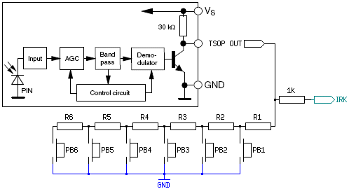
I am working with a msp430f2274 and I am doing an exercise with a hex keypad. I have the outputs working just fine, but I am having difficulty reading the input signals. The way I figured is that the best way to do this is by scanning the ADC values of each pin. (P3, P4, P5) I believe my main issue is not knowing how to trigger the sampling for each individual input pin, and I don't know if I need a slight delay in order to reset the ADC. I have constructed a sample code to demonstrate what I am trying to do for sampling.
#include "msp430f2274.h"
int main(void)
{
//Initialize ADC & WDT
WDTCTL = WDTPW + WDTHOLD; // Stop WDT
ADC10CTL0 = ADC10SHT_2 + ADC10ON + ADC10IE; // ADC10ON, interrupt enabled
ADC10AE0 |= 0x07; // P2.2,1,0 ADC10 option select
P1DIR |= 0x01; // Set P1.0 to output direction
//End of Initialization
//Start sampling loop
for (;;)
{
//Sample P3
ADC10CTL0 |= ENC + ADC10SC; // Sampling and conversion start P3
__bis_SR_register(CPUOFF + GIE); // LPM0, ADC10_ISR will force exit
if (ADC10MEM < 0x238)
//do something
//Sample P4
//Command for sample for P4?
__bis_SR_register(CPUOFF + GIE); // LPM0, ADC10_ISR will force exit
if (ADC10MEM < 0x238)
// Do something
//Sample P5
//Command to sample start for P5?
__bis_SR_register(CPUOFF + GIE); // LPM0, ADC10_ISR will force exit
if (ADC10MEM < 0x238)
//do something
}
}
// ADC10 interrupt service routine
#pragma vector=ADC10_VECTOR
__interrupt void ADC10_ISR(void)
{
__bic_SR_register_on_exit(CPUOFF); // Clear CPUOFF bit from 0(SR)
}