Because of the Thanksgiving holiday in the U.S., TI E2E™ design support forum responses may be delayed from November 25 through December 2. Thank you for your patience.

This thread has been locked.

If you have a related question, please click the "Ask a related question" button in the top right corner. The newly created question will be automatically linked to this question.

SPI read out problem with MSP430G2553 launchpad

Other Parts Discussed in Thread: MSP430G2553

Hello,

We are interfacing AT25128B EEPROM with MSP430G2553 launchpad board over SPI. We are using CCS version 5.1 to develop our code. 

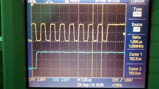
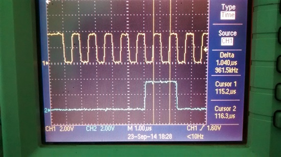
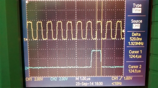
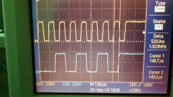
We are trying to write a data on one location and read from same location to test EEPROM. But we didn't get same value after reading that same location. We always get 0xFF or 0x00 value after reading that location. Our SPI configuration is clock 1 MHz and mode 3. We have also checked with SPI mode 0 but same problem occured. We have captured waveforms of SPI clock and MOSI pins and noted that all sequences are correct. I have attached our code and waveforms here.

Please look at my code and make a suggestion as what the problem might be, I would greatly appreciate it.

5417.main.c
/*
 *
 * SPI Connections:
 * CS   - P1.4 (Active Low)
 * SCLK - P1.5
 * MOSI - P1.7
 * MISO - P1.6
 *
 * UART TX: P1.1
 * UART RX: P1.2
 *
 */

#include <msp430.h> 
#include "uart.h"

//opcodes
#define WREN  	6
#define WRDI  	4
#define RDSR  	5
#define WRSR  	1
#define READ  	3
#define WRITE 	2

#define DLY		80000	// 5 MS
#define DATA	0x55

char recv_data;


void spi_write(char byte)
{
	UCB0TXBUF = byte;
	while (!( IFG2 & UCB0TXIFG));
}

char spi_read(void)
{
	while (!(IFG2 & UCB0RXIFG));   // USCI_b0 RX Received?
	return(UCB0RXBUF);
}

void write_enable(void)
{
	P1OUT &= ~BIT4;			// Enable Device
	_delay_cycles(DLY);
	spi_write(WREN);
	_delay_cycles(DLY);
	P1OUT |= BIT4;			// Disable Device
}

void write_disable(void)
{
	P1OUT &= ~BIT4;			// Enable Device
	_delay_cycles(DLY);
	spi_write(WRDI);
	_delay_cycles(DLY);
	P1OUT |= BIT4;			// Disable Device
}

void isDeviceReady(void)
{
	char status;

	P1OUT &= ~BIT4;			// Enable Device
	//_delay_cycles(DLY);
	spi_write(RDSR);
	spi_write(0xFF);
	status = spi_read();
	uart_put(status);		// Debug point - Send Status register value on UART
	P1OUT |= BIT4;			// Disable Device
	//_delay_cycles(DLY);

	while(status & 0x01);	// Wait to complete write cycle
}

void eeprom_write(void)
{
	write_enable();			// Enable Write cycle

	P1OUT &= ~BIT4;			// Enable Device
	_delay_cycles(DLY);
	
	spi_write(WRITE);
	spi_write(0x00);		// MSB Address
	spi_write(0xAA);		// LSB Address
	spi_write(DATA);		// Data
	
	P1OUT |= BIT4;			// Disable Device
	isDeviceReady();
	_delay_cycles(DLY);

	write_disable();		// Disable write
}

char eeprom_read(void)
{
	char ch = 1;

	P1OUT &= ~BIT4;			// Enable Device
	_delay_cycles(DLY);
	
	spi_write(READ);
	spi_write(0x00);		// MSB Address
	spi_write(0xAA);		// LSB Address

	spi_write(0xFF);		// Dummy data
	ch = spi_read();
	
	uart_put(ch);			// Debug point
	
	P1OUT |= BIT4;			// Disable Device
	_delay_cycles(DLY);

	return(ch);
}

void clockConfig(void)
{
	// configure the CPU clock (MCLK)
	// to run from DCO @ 16MHz and SMCLK = DCO / 4
	BCSCTL1 = CALBC1_16MHZ; // Set DCO
	DCOCTL = CALDCO_16MHZ;
	BCSCTL2= DIVS_2 + DIVM_0; 	// divider = 4 for SMCLK and 1 for MCLK
}

void spi_init(void)
{
	// set the pin mode 3 for pins 5,6 & 7 of port 1 (USCI mode)
	P1SEL |= BIT5 + BIT6 + BIT7; // low bit = 1 for pins 5,6 and 7 BIT 3 is 0 (CS via GPIO)
	P1SEL2 |= BIT5 + BIT6 + BIT7; // high bit = 1 for pins 5,6 and 7 BIT 3 is 0 (CS via GPIO)

	P1DIR |= BIT4; // p1.4 set to output to drive CS
	P1OUT |= BIT4; // pull p1.4 to high - CS high -> chip is disabled

	UCB0CTL1 = UCSWRST; 
	// synchronous (=SPI) master 3 wire SPI, clock polarity HIGH at Idle
	// SPI mode 3
	UCB0CTL0 |= UCCKPL | UCMST | UCSYNC | UCMSB | UCMODE_0;

	UCB0CTL1 |= UCSSEL_2; //use SCLK : 4MHz

	// set baud rate = SMCLK, divide by 2
	UCB0BR0 = 0x04;		// SPI clock : 1 MHz
	UCB0BR1 = 0;
	UCB0CTL1 &= ~UCSWRST; // ** Initialize USCI **
}

void uart_init(void)
{
	P1SEL |= RXD + TXD ; // P1.1 = RXD, P1.2=TXD
	P1SEL2 |= RXD + TXD ; // P1.1 = RXD, P1.2=TXD

	UCA0CTL1 = UCSWRST; 	// reset
	UCA0CTL1 |= UCSSEL_2; 	// SMCLK
	UCA0BR0 = 0xA0;			// 9600 baud rate
	UCA0BR1 = 0x01; 			
	UCA0MCTL = UCBRS2 | UCBRS1;	
	UCA0CTL1 &= ~UCSWRST; // **Initialize USCI state machine**
}

void uart_put(char byte)
{
	UCA0TXBUF = byte;
	while (!( IFG2 & UCA0TXIFG));
}

/*
 * main.c
 */
int main(void)
{
    WDTCTL = WDTPW | WDTHOLD;	// Stop watchdog timer

    clockConfig();
    uart_init();
    spi_init();
	
	// Set LED Direction
    P1DIR |= BIT0;
    P1OUT |= BIT0;

    uart_put('A');

	// Write EEPROM
	eeprom_write();
	
	// Read EEPROM
	recv_data = eeprom_read();

	// Check received data is same as written data
	if(recv_data == DATA)
	{
		P1OUT &= ~BIT0;
	}
	else if(recv_data == 0xFF)
	{
		P1OUT |= BIT0;
	}
	else
	{
		P1OUT ^= BIT0;
	}

	while(1)
	{
	}
	
}

Thanks,

Nipam

  • Nipam,

    From first glance, it looks like you may need to invert  the SPI clock.

    According to the datasheet for the EPROM, the inactive state is low.

    According to the images, it looks like the inavtive state is hi.


    -Jason

  • Hello Jason,

    Thanks for your response.

    Because of SPI mode 3, SPI clock is High at Idle time. As per datasheet, EEPROM supports both SPI mode 0 and 3. We have tried with both SPI modes. But same result occured with both SPI modes. Captured waveforms show SPI mode 3.

    I have doubt about our code. Somewhere we did mistake or missing something in the code. Can you please look into our code? 

    Thanks,

    Nipam


  • This information will not solve your problem, but I will give you this advice anyway:

    void isDeviceReady(void)
    {
      char status;
    
      P1OUT &= ~BIT4;            // Enable Device
      //_delay_cycles(DLY);
      spi_write(RDSR);
      spi_write(0xFF);
      status = spi_read();
      uart_put(status);          // Debug point - Send Status register value on UART
      P1OUT |= BIT4;             // Disable Device
      //_delay_cycles(DLY);
    
      while(status & 0x01);      // Wait to complete write cycle
    }

    Your last line is potentially dangerous because if your EEPROM would answer that it is not ready, having bit 0x01 set then your program will last there forever. Your status variable cannot change during the while-loop.

  • And here is probably a solution for your problem:

    You are working with a 2 channel oscilloscope watching CLK and data, but you do not see the chip-select line - this one is important. So you should have a look at CLK and CS making sure CS does not go high again too early.

    The problem in your code could be the polling of UCB0TXIFG. Look at this code snippet:

    void write_enable(void)
    {
      P1OUT &= ~BIT4;       // Enable Device
      _delay_cycles(DLY);
      spi_write(WREN);
      _delay_cycles(DLY);
      P1OUT |= BIT4;        // Disable Device
    }
    

    You are setting CS low and send your data. After each byte you are polling UCB0TXIFG before sending the next byte. That is OK, but after the last byte this procedure won't work beacause UCB0TXIFG is set again after the byte is moved from the TX-buffer to the shift-register and not after the transmission is complete. You are using a delay, OK, but to really make sure everything has been finished you should at least poll the UCBUSY-flag before setting CS high again. The even better solution would be to work with interrupts, setting CS high again after RXIFG of the last byte causes an interrupt. But for the moment it's OK.

    Setting CS high again too early is a problem I often see when looking at "problem codes". You could at least give it a try.

    Dennis

  • Hello Dennis,

    Thanks for your inputs.

    I will update you ASAP after checking your suggestions. Also I will share CS pin and Clock waveforms with you.

    Thanks again.

    Regards,

    Nipam

  • Hello Dennis,

    Thanks for your suggestion. EEPROM works fine now.

    The problem is we forget to connect capacitor between VCC and GND pins of EEPROM IC. After connecting capacitor and checking UCBUSY bit in UCB0STAT register as per your suggestion, it works fine. I have attached my working code here.

    Thanks again for all suggestions to all.

    2134.main_eeprom.c
    /*
     * SPI Connections:
     * CS   - P1.4 (Active Low)
     * SCLK - P1.5
     * MOSI - P1.7
     * MISO - P1.6
     *
     * 80000 - 50 ms
     */
    
    #include <msp430.h>
    
    //opcodes
    #define WREN  	6
    #define WRDI  	4
    #define RDSR  	5
    #define WRSR  	1
    #define READ  	3
    #define WRITE 	2
    
    #define DLY		16000	//1 MS		//80000	// 5 MS
    #define DATA	0x50
    
    char recv_data;
    
    
    void spi_write(char byte)
    {
    	UCB0TXBUF = byte;
    	while (!( IFG2 & UCB0TXIFG));
    }
    
    char spi_read(void)
    {
    	while (!(IFG2 & UCB0RXIFG));   // USCI_b0 RX Received?
    	return(UCB0RXBUF);
    }
    
    void write_enable(void)
    {
    	P1OUT &= ~BIT4;			// Enable Device
    	_delay_cycles(DLY);
    	spi_write(WREN);
    	_delay_cycles(DLY);
    	P1OUT |= BIT4;			// Disable Device
    }
    
    void write_disable(void)
    {
    	P1OUT &= ~BIT4;			// Enable Device
    	_delay_cycles(DLY);
    	spi_write(WRDI);
    	_delay_cycles(DLY);
    	P1OUT |= BIT4;			// Disable Device
    }
    
    void isDeviceReady(void)
    {
    	unsigned char status;
    
    	P1OUT &= ~BIT4;			// Enable Device
    
    	spi_write(RDSR);
    	while((UCB0STAT & UCBUSY));		// Check busy or not
    
    	spi_write(0xFF);
    
    	status = spi_read();
    
    	uart_put(status);
    	P1OUT |= BIT4;			// Disable Device
    
    	while(status & 0x01);
    }
    
    void eeprom_write(void)
    {
    	write_enable();
    
    	P1OUT &= ~BIT4;			// Enable Device
    	_delay_cycles(DLY);
    
    	spi_write(WRITE);
    
    	spi_write(0x00);		// MSB Address
    
    	spi_write(0xAA);		// LSB Address
    
    	spi_write(DATA);
    	while((UCB0STAT & UCBUSY));		// Wait if Transmit process is busy
    
    	_delay_cycles(DLY);
    	P1OUT |= BIT4;			// Disable Device
    
    	write_disable();
    	_delay_cycles(100);
    }
    
    char eeprom_read(void)
    {
    	char ch = 1;
    
    	P1OUT &= ~BIT4;			// Enable Device
    	_delay_cycles(DLY);
    
    	spi_write(READ);
    
    	spi_write(0x00);		// MSB Address
    
    	spi_write(0xAA);		// LSB Address
    
    	spi_write(0xFF);
    	while((UCB0STAT & UCBUSY));		// Wait if Transmit process is busy
    
    	ch = spi_read();
    
    	_delay_cycles(DLY);
    	P1OUT |= BIT4;			// Disable Device
    
    	return(ch);
    }
    
    void clockConfig(void)
    {
    	// configure the CPU clock (MCLK)
    	// to run from DCO @ 16MHz and SMCLK = DCO / 4
    	BCSCTL1 = CALBC1_16MHZ; // Set DCO
    	DCOCTL = CALDCO_16MHZ;
    	BCSCTL2= DIVS_2 + DIVM_0; 	// divider=4 for SMCLK and 1 for MCLK
    }
    
    void spi_init(void)
    {
    	// set the pin mode 3 for pins 5,6 & 7 of port 1 (USCI mode)
    	P1SEL |= BIT5 + BIT6 + BIT7; // low bit = 1 for pins 5,6 and 7 BIT 3 is 0 (CS via GPIO)
    	P1SEL2 |= BIT5 + BIT6 + BIT7; // high bit = 1 for pins 5,6 and 7 BIT 3 is 0 (CS via GPIO)
    
    	P1DIR |= BIT4; // p1.4 set to output to drive CS
    	P1OUT |= BIT4; // pull p1.4 to high - CS high -> chip is disabled
    
    	UCB0CTL1 = UCSWRST;
    
    	// synchronous (=SPI) master 3 wire SPI, clock polarity Low at idle
    	// SPI mode 0
    	UCB0CTL0 |= UCCKPH | UCMST | UCSYNC | UCMSB | UCMODE_0;
    
    	UCB0CTL1 |= UCSSEL_2; //use SCLK : 4MHz
    
    	// set baud rate = SMCLK, divide by 4, SPI Clock Freq : 1 MHz
    	UCB0BR0 = 0x04;
    	UCB0BR1 = 0;
    	UCB0CTL1 &= ~UCSWRST; // ** Initialize USCI **
    }
    
    void uart_init(void)
    {
    	P1SEL |= RXD + TXD ; // P1.1 = RXD, P1.2=TXD
    	P1SEL2 |= RXD + TXD ; // P1.1 = RXD, P1.2=TXD
    
    	UCA0CTL1 = UCSWRST; 	// reset
    	UCA0CTL1 |= UCSSEL_2; 	// SMCLK
    	UCA0BR0 = 0xA0;			// 9600 baud rate		// 0x08; // 1MHz 115200
    	UCA0BR1 = 0x01; 			// 1MHz 9600
    	UCA0MCTL = UCBRS2 | UCBRS1;	//UCBRF_1 | UCOS16;	// 9600
    	UCA0CTL1 &= ~UCSWRST; // **Initialize USCI state machine**
    	//UC0IE |= UCA0RXIE; // Enable USCI_A0 RX interrupt
    }
    
    void uart_put(char byte)
    {
    	UCA0TXBUF = byte;
    	while (!( IFG2 & UCA0TXIFG));
    }
    
    /*
     * main.c
     */
    int main(void)
    {
        WDTCTL = WDTPW | WDTHOLD;	// Stop watchdog timer
    
        clockConfig();
        uart_init();
        spi_init();
    
        // Set LED direction for Debug
        P1DIR |= BIT0;
        P1OUT |= BIT0;
    
        uart_put('A');
    
        // Write a byte on specific location
    	eeprom_write();
    
    	// Read a byte from specific location
    	recv_data = eeprom_read();
    
    	uart_put(recv_data);
    
    	if(recv_data == DATA)	// Check read data is same as written data
    	{
    		P1OUT &= ~BIT0;
    		uart_put('a');
    	}
    	else if(recv_data == 0x00)
    	{
    		P1OUT &= ~BIT0;
    	}
    	else if(recv_data == 0xFF)
    	{
    		P1OUT |= BIT0;
    	}
    	else
    	{
    		P1OUT ^= BIT0;
    	}
    
    	while(1);
    }
    

    Thanks,

    Nipam

**Attention** This is a public forum