


Other Parts Discussed in Thread: MSP430F2272
I want to use ADC12 to measure battery voltage on MSP430 F5435.
But I don't know how to getting started. Could anyone give some suggestions or
example code? Thanks

This thread has been locked.
If you have a related question, please click the "Ask a related question" button in the top right corner. The newly created question will be automatically linked to this question.
Other Parts Discussed in Thread: MSP430F2272
I want to use ADC12 to measure battery voltage on MSP430 F5435.
But I don't know how to getting started. Could anyone give some suggestions or
example code? Thanks
Hi Alvin,
have a look at the code examples for F543x series http://www.ti.com/lit/zip/slac166. Have a loot at the Read-Me file (http://focus.ti.com/lit/ml/slaa439/slaa439.pdf) for details on the enclosed samples.
Rgds
aBUGSworstnightmare
I am using an MSP430F2272, but the concept is the same.
I divide the battery voltage by 2 using 10K, 1% resistors. I also use the 2.5 volt reference.
Then I use the following code to get the voltage:
battery_voltage = Read_ADC_Ch(BATTERY_CH); // defined as channel 5 on my board
battery_voltage = (battery_voltage * 250)/4095;
battery_voltage = battery_voltage * 2; //using a resistor divider
Note that the 2272 has an ADC10, but I oversample and divide to get a 12 bit reading. That's why I multiply by 4095.
Leaving the divider connected uses power, so on my circuit I isolate them using FETs, only turning them on for the read.

Hmmm, do you think oversampling a static signal gives a higher resolution? And do you think you actually need this resulution? I don't.
The battery voltage is at the upper limit of the ADC range. And with an internal reference of +-3%, the upper 8 bits of the ADC reading are already beyond any sane meaning (0.4%). Not to mention the additional error introduced by the 1% resistors. The additional bits are only of use if the measured signal is very small. Even then will oversampling be of no help, as even hundred times the same divided by 100 is no more precise than one measurement. Oversampling is only usefull if you have a fast changing signal. Then you can interpolate values in between by building an average. Still the noise you sample might be higher than the value of your additional bits.
On the MSPs, only 6-7 bits down from the highest set bit are meaningful, the rest below is rubbish. Having 10 or even 12 bit ADC adds to the dynamic range, but precision at full range isn't higher than with an 8 bit ADC.
But back to the original problem. The voltage divider, built by two resistors between VCC and VSS with their middle point connected tot he ADC input, needs to break down battery voltage to something below reference which is 2.5V usually, but maybe 1.5V need to be used if you're using a low voltage setup with VccMSP below 3V. So in case of any battery voltage above 5V (and even slightly below, so 3*AA might be already too high), it must be something higher than just 1:1. if the resistors are from the same charge, the tolerance isn't a problem, at least for 1:1 division, as 10k:10k is the same as 11k:11k and resistors from the same charge usually have their tolerance tending the same magnitude and direction. So if 2:1 is required, two resistors in a row are better than one of twice the size (not mentioning the fact that 2:1 values are not in every standard parts box).
If you just want to know when the battery voltage drops below what you need for running the MSP, the ADC has a VCC/2 channel with on-die divider resistors. This way you can see when the supply voltage begins to drop and issue an alert. Keep in mind that (as already stated) an external divider adds to the power consumption. This might be an issue for some applications. But a FET not only requires a port pin, it also adds to the error. And, depending on the FET used, this error might be even nonlinear. And, of course, the reference tolerance requires some tolerance for your alert threshold too.
Finally, after this theoretical stuff, here a code example:
unsigned long tOffset;
unsigned int tFactor;
void InitAD(void){
unsigned char ref = 0;
P6SEL|= 0xff; // disable digital I/O on port 6
P7SEL|= 0xf0; // and port 7
P6REN = 0; // disable pullups on port 6
P7REN&= 0x0f); // and port 7
ADC12CTL0 = ADC12ON; // deactivate ADC12
ADC12CTL1 = 0;
ADC12CTL2 = 0;
ADC12IE = 0; //deactivate interrupts (free-running conversion)
ADC12CTL0 |= ADC12REFON;
ADC12CTL0 |= ADC12REF2_5V;
ref = ADC12SREF_VREF_AVSS ;
ADC12CTL0 |= ADC12SHT0_64 | ADC12SHT1_128 | ADC12MSC; // 64+13 clk cycles conv.time * 8 ch + 128+13 cycles *6 ch = 2.73 conversion cycles/ms @ 16MHz/4, 16µs/32µs s&h -> 31250/15625Hz fG
ADC12CTL1 |= ADC12_R_SEQUENCE | ADC12SSEL_MCLK | ADC12DIV_0 | ADC12SHP | ADC12SHS_ADC12SC | ADC12CSTARTADD_0;
ADC12CTL2 |= /*ADC12SR |*/ ADC12RES_12BIT | ADC12PDIV;
ADC12MCTL0=ref|ADC12INCH_0; // Port A0 against selected reference
ADC12MCTL1=ref|ADC12INCH_1; // Port A1 against selected reference
ADC12MCTL2=ref|ADC12INCH_2; // Port A2 against selected reference
ADC12MCTL3=ref|ADC12INCH_3; // Port A3 against selected reference
ADC12MCTL4=ref|ADC12INCH_4; // Port A4 against selected reference
ADC12MCTL5=ref|ADC12INCH_5; // Port A5 against selected reference
ADC12MCTL6=ref|ADC12INCH_6; // Port A6 against selected reference
ADC12MCTL7=ref|ADC12INCH_7; // Port A7 against selected reference
ADC12MCTL8=ref|ADC12INCH_12; // Port A12 against selected reference
ADC12MCTL9=ref|ADC12INCH_13; // Port A13 against selected reference
ADC12MCTL10=ref|ADC12INCH_14; // Port A14 against selected reference
ADC12MCTL11=ref|ADC12INCH_15; // Port A15 against selected reference
ADC12MCTL12=ADC12SREF_VREF_AVSS|ADC12INCH_TEMP; // internal TEMP sensor against internal reference (calibration available)
ADC12MCTL13=ref|ADC12INCH_VCC2| ADC12EOS; // VCC/2 against selected reference, end of sequence
// calculate tFactor/tOffset for temp channel
tFactor = (((550UL)<<12)+150)
/(
(*((unsigned int *)(0x1a1e + ((_SYSTEM_AD_REF & 1)?6:0))))
-(*((unsigned int *)(0x1a1c + ((_SYSTEM_AD_REF & 1)?6:0))))
); // 550 is ref temp diff (1/10°), +150 is added for cheap rounding (calibration points are ~300 apart)
tOffset = ((unsigned long)(*((unsigned int *)(0x1a1c +((_SYSTEM_AD_REF & 1)?6:0))))*tFactor)-(300UL<<12);
ADC12CTL0 |= ADC12ENC | ADC12SC;
}
After this initialisation ( a simplified version, my original code allows defining of reference and actually used channels), the ADC is constantly measuring all 12 ADC inputs as well as the internal TEMP sensor and the VCC/2 reading.
The actual values are retrieved by these formulae:
ADIN[i]=ADC12MEM[i]; // save current ADC12MEM value
if(ADIN[i]<ADOFFSET[i])ADIN[i]=0; else ADIN[i]-=ADOFFSET[i]; // remove calibrated offset (and ensure it doesn't go negative)
ADIN[i]=((((long)(ADIN[i])*(long)(ADFACTOR[i])))>>14); // do calibration stuff here
Temperature=((((long)ADC12MEM[12]*tFactor)-tOffset)>>12);
Voltage=(ADC12MEM[13]*250L)>>11; // 1/2 VCC -> 100* VCC (VCC * 10mV)
The temperature contains the internal temperature sensors reading in 1/10 °C (calculated using the calibration values in the processors TLV structure), voltage is in 10mV steps (e.g. 300 = 3V VccMSP) , ADOFFSET[] is an array holding an offset value for each channel (default value 0), ADFACTOR[] is an array with calibration factor values for the linear error. Default value is 1000 (actually 1000.2442). The results in ADIN[i] are measured voltage in 10mV steps. Note that there are no divisions (divisions are SLOOOOW).
For the 1/2 battery voltage level simply set ADFACTOR[x] to 2000 etc.
Not that the used constants might not be available for your compiler. I created the header file for the ADC12A myself, as there was none for MSPGCC. I tried to match the definitions in the TI datasheets and the dofinitions in previous datasheets for the ADC12 (non-A) as close as possible, but there might be differences.
If you need higher precision than the internal voltage reference gives, you can use a TS431BC, a shunt regulator with 2.495V +-0.5% and 50ppm Temperature coefficient., available in TO92 (-T) as well as SOT23 (-X). It requires, however, a minimum shunt current of 1mA, so it should be sourced by an MSP port pin if this is an issue. With 0.22Ohm dynamic resistance, it is a very stable voltage reference even for greater currents (up to 100mA). And it costs only a few cents.

Oversampling the divided battery voltage is not required. I just happen to use the same routine to check it as I use for the signals that do.
My application is a wireless gauge that has a high duty cycle. The radio uses a fair number of milliamps. I need to know when to tell the user that the unit needs to go in the charging cradle.

Thanks to everyone from your suggestions. Maybe I don't need oversampling to get higher resolution.
I have never used ADC as any application. I felt a bit for confusion even read some documents.
It has 16 channels on MSP430 F5435. Which channel could be used to measure battery voltage?
Battey voltage is connected to A12 as bellow. Is it correct?
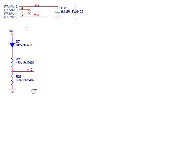
Whether this is correct depends on the circumstances.
The voltage you see at A12 is
((Vbatt-Vd7)*68)/(47+68)
Depending on D7 the maximum Vbatt you can measure it 4,3..4,9V. Also, the use of a diode adds a non-linear offset voltage (Vd7) which depends on teh current running through D7. Since the current is very low (~40µA), the forward voltage of the diode changes greatly and hyperbolically with the current (which depends on Vbatt). I wouldn't recomment it.
Another thing is that you have a limited input impedance (thus input current) on A12. This lies in parallel to R27. With R27 being relatively high, this influence may lower the resulting resistance to GND and therefore affect the R27/(R28+R27) term. The division factor is greater than expected. This of course can be removed by calibration.
The leakage current through C17 is another non-linear current added in parallel to R27. You don't really need it and if you want some noise decoupling/low pass on A12, with these resistor values 10nF is big enough. But go for a type with low leakage current.
It all depends on how a exact reading you need. If you just need to know, with substancial tolerance, whether a certain threshold voltage is reached, all this is void and you can go with this without further considerations. Then it is good enough to precalculate the AD12 reading that will eb your threshold, so no calculations in the software are needed. Just compare the ADCMEM register content with your precalculated threshold value. You may even choose to program the ADC for 10 or 8 bit conversion to preserve a few microamperes.
As for your document question: yes, teh ADC12A has 16 channels. The first 12 are identical to the ones available on device with the ADC12 (non-A). Channel 0..7 is connected to A0..7, then follow 4 internal channels, measuring VCC/2, TEMP, Vref and GND (the latter two can be used with a temporarily attached external reference voltage to calibrate the internal voltage reference). Then the ADC12A has another 4 channels (12..15) attached to A12..15. As you can see, there are no A8..11 pins.
The conversion memory locations (also 16) are NOT fixed to any input channel. It depends on your programming of the ADC12A which and how many external or internal channels are stored on which ADCMEM register. So you can set up the ADC12A to convert only 2 inputs up to eight times (or one up to 16 times in a row) in alternating order before you get an ADC interrupt, then you have 4 (8) values for calculating an average (low pass, de-noise). It's up to you. In my code example I reordered teh external A12..A15 channels to ADCMEM[8..1] and added only the VCC/2 and TEMP, since the other two internal channels are of no use in normal operation. So two less conversions are done before the cycle is repeated. (I leave it free-running and just read all 14 memory locations every ms, but our devices are attache dto AC power all the time, so teh additional enegy consumption of constanlty free-running conversions really does not matter). You can go for one-shot single conversion if you need a voltage reading, to preserve energy.
**Attention** This is a public forum
