This thread has been locked.

If you have a related question, please click the "Ask a related question" button in the top right corner. The newly created question will be automatically linked to this question.

Unexpected RESET during DMA-to-UART with Timer_A

Other Parts Discussed in Thread: MSP430FR5969, MSP430WARE

I have encountered a couple of problems.  I am using the MSP430FR5969 LaunchPad.  I have a simple program that transfers contents of an array to the UART Tx buffer using DMA.  At the same time, the main loop wakes up periodically from LPM3 using Timer A.

The first, and less troubling problem, is that the DMA initiates without ever sending an initial trigger.  The DMA trigger source is set to the UCA1TXIFG.  I should have to manually write the first byte to the UART Tx Buffer to trigger the DMA, but somehow the DMA gets triggered without doing this.

The second, and more concerning problem, is that the mcu resets.  The shorter the Timer A period and the faster the UART baud rate the faster the reset occurs.  I have tried a number of baud rates and timer periods, and the reset always eventually occurs.

The WDT is disabled.  I have tried including an ISR for every vector, but the reset still occurs.  I am using the MSP430Ware driverLib.  It makes no difference if the project is build with the TI or GNU compiler.

The only enabled interrupt is the Timer A interrupt.  All that is done in the ISR is clearing the interrupt flag and exiting LPM3.  I have tried a number of variations with no change.

Any help, suggestions, ideas would be greatly appreciated.  This appears to be a significant problem.  Code follows.

Thanks,

Warren

int main(void)
{
	uint8_t s1, s2;

	WDTCTL = WDTPW | WDTHOLD;	// Stop watchdog timer

	// look for S1 (to catch unexpected reset)
	InitPushbuttons(PUSHBUTTON_BOTH, 0);
	getPushbuttons(&s1, &s2);

	Init_GPIO();
	Init_Clock();
    Init_Serial();
    Init_DMA();


    // catch unexpected reset if S1 was not pressed
	if(s1 != 0)
		ABORT;

	// enable source DMA
	DMA_enableTransfers(DMA_CHANNEL_0);

	// kick off dma by manually sending first byte
	//EUSCI_A_UART_transmitData(EUSCI_A1_BASE, 0x99);

	// configure Timer A (at 32.768 KHz clock)
	TIMER_A_configureUpMode( TIMER_A3_BASE,
			TIMER_A_CLOCKSOURCE_ACLK ,
			TIMER_A_CLOCKSOURCE_DIVIDER_1,
			0x0080,
			TIMER_A_TAIE_INTERRUPT_ENABLE,
			TIMER_A_CCIE_CCR0_INTERRUPT_DISABLE,
			TIMER_A_DO_CLEAR);

	greenLedOn();

	// start the timer
	TIMER_A_startCounter(
			TIMER_A3_BASE,
			TIMER_A_UP_MODE);

	while(1)
	{

		// Enter LPM3
		__bis_SR_register(LPM3_bits | GIE);

		greenLedToggle();
		redLedToggle();

		// if timer was stopped in ISR, restart timer
		TIMER_A_startCounter(
				TIMER_A3_BASE,
				TIMER_A_UP_MODE);
	}
	return(0);
}

#if defined (__TI_COMPILER_VERSION__) || defined (__IAR_SYSTEMS_ICC__)
#pragma vector=TIMER3_A1_VECTOR
__interrupt void TIMER3_A1_ISR(void)
#elif defined(__GNUC__)
void TIMER3_A1_ISR(void) __attribute__ ((interrupt(TIMER3_A1_VECTOR)));
void TIMER3_A1_ISR(void)
#else
#error Compiler not supported!
#endif
{
	unsigned int taxiv;

	// stop the timer
	TIMER_A_stop(TIMER_A3_BASE);

	// clear the interrupt
	taxiv = HWREG16(TA3IV);

	// exit LPM3
	__bic_SR_register_on_exit(LPM3_bits);
}

Support code:

#define DMA_SIZE 128
const unsigned char gBits[DMA_SIZE] = {
		0x55, 0x55, 0x55, 0x55, 0x55, 0x55, 0x55, 0x55, 0x55, 0x55, 0x55, 0x55, 0x55, 0x55, 0x55, 0x55,
		0x55, 0x55, 0x55, 0x55, 0x55, 0x55, 0x55, 0x55, 0x55, 0x55, 0x55, 0x55, 0x55, 0x55, 0x55, 0x55,
		0x55, 0x55, 0x55, 0x55, 0x55, 0x55, 0x55, 0x55, 0x55, 0x55, 0x55, 0x55, 0x55, 0x55, 0x55, 0x55,
		0x55, 0x55, 0x55, 0x55, 0x55, 0x55, 0x55, 0x55, 0x55, 0x55, 0x55, 0x55, 0x55, 0x55, 0x55, 0x55,
		0x55, 0x55, 0x55, 0x55, 0x55, 0x55, 0x55, 0x55, 0x55, 0x55, 0x55, 0x55, 0x55, 0x55, 0x55, 0x55,
		0x55, 0x55, 0x55, 0x55, 0x55, 0x55, 0x55, 0x55, 0x55, 0x55, 0x55, 0x55, 0x55, 0x55, 0x55, 0x55,
		0x55, 0x55, 0x55, 0x55, 0x55, 0x55, 0x55, 0x55, 0x55, 0x55, 0x55, 0x55, 0x55, 0x55, 0x55, 0x55,
		0x55, 0x55, 0x55, 0x55, 0x55, 0x55, 0x55, 0x55, 0x55, 0x55, 0x55, 0x55, 0x55, 0x55, 0x55, 0x55
};


void Init_GPIO()
{
    // Set all GPIO pins to output low for low power
    GPIO_setOutputLowOnPin(GPIO_PORT_P1, GPIO_PIN0|GPIO_PIN1|GPIO_PIN2|GPIO_PIN3|GPIO_PIN4|GPIO_PIN5|GPIO_PIN6|GPIO_PIN7);
    GPIO_setOutputLowOnPin(GPIO_PORT_P2, GPIO_PIN0|GPIO_PIN1|GPIO_PIN2|GPIO_PIN3|GPIO_PIN4|GPIO_PIN5|GPIO_PIN6|GPIO_PIN7);
    GPIO_setOutputLowOnPin(GPIO_PORT_P3, GPIO_PIN0|GPIO_PIN1|GPIO_PIN2|GPIO_PIN3|GPIO_PIN4|GPIO_PIN5|GPIO_PIN6|GPIO_PIN7);
    GPIO_setOutputLowOnPin(GPIO_PORT_P4, GPIO_PIN0|GPIO_PIN1|GPIO_PIN2|GPIO_PIN3|GPIO_PIN4|GPIO_PIN5|GPIO_PIN6|GPIO_PIN7);
    GPIO_setOutputLowOnPin(GPIO_PORT_PJ, GPIO_PIN0|GPIO_PIN1|GPIO_PIN2|GPIO_PIN3|GPIO_PIN4|GPIO_PIN5|GPIO_PIN6|GPIO_PIN7|GPIO_PIN8|GPIO_PIN9|GPIO_PIN10|GPIO_PIN11|GPIO_PIN12|GPIO_PIN13|GPIO_PIN14|GPIO_PIN15);

    GPIO_setAsOutputPin(GPIO_PORT_P1, GPIO_PIN0|GPIO_PIN1|GPIO_PIN2|GPIO_PIN3|GPIO_PIN4|GPIO_PIN5|GPIO_PIN6|GPIO_PIN7);
    GPIO_setAsOutputPin(GPIO_PORT_P2, GPIO_PIN0|GPIO_PIN1|GPIO_PIN2|GPIO_PIN3|GPIO_PIN4|GPIO_PIN5|GPIO_PIN6|GPIO_PIN7);
    GPIO_setAsOutputPin(GPIO_PORT_P3, GPIO_PIN0|GPIO_PIN1|GPIO_PIN2|GPIO_PIN3|GPIO_PIN4|GPIO_PIN5|GPIO_PIN6|GPIO_PIN7);
    GPIO_setAsOutputPin(GPIO_PORT_P4, GPIO_PIN0|GPIO_PIN1|GPIO_PIN2|GPIO_PIN3|GPIO_PIN4|GPIO_PIN5|GPIO_PIN6|GPIO_PIN7);
    GPIO_setAsOutputPin(GPIO_PORT_PJ, GPIO_PIN0|GPIO_PIN1|GPIO_PIN2|GPIO_PIN3|GPIO_PIN4|GPIO_PIN5|GPIO_PIN6|GPIO_PIN7|GPIO_PIN8|GPIO_PIN9|GPIO_PIN10|GPIO_PIN11|GPIO_PIN12|GPIO_PIN13|GPIO_PIN14|GPIO_PIN15);

    // Set PJ.4 and PJ.5 as Primary Module Function Input, LFXT.
    GPIO_setAsPeripheralModuleFunctionInputPin(
           GPIO_PORT_PJ,
           GPIO_PIN4 + GPIO_PIN5,
           GPIO_PRIMARY_MODULE_FUNCTION
           );


    // Disable the GPIO power-on default high-impedance mode
    // to activate previously configured port settings
    PMM_unlockLPM5();
}

void Init_Clock()
{
    // Set DCO frequency to 8 MHz
    CS_setDCOFreq(CS_DCORSEL_0, CS_DCOFSEL_6);
    //Set external clock frequency to 32.768 KHz
    CS_setExternalClockSource(32768, 0);
    //Set ACLK=LFXT
    CS_clockSignalInit(CS_ACLK, CS_LFXTCLK_SELECT, CS_CLOCK_DIVIDER_1);
    // Set SMCLK = DCO with frequency divider of 1
    CS_clockSignalInit(CS_SMCLK, CS_DCOCLK_SELECT, CS_CLOCK_DIVIDER_1);
    // Set MCLK = DCO with frequency divider of 1
    CS_clockSignalInit(CS_MCLK, CS_DCOCLK_SELECT, CS_CLOCK_DIVIDER_1);
    //Start XT1 with no time out
    CS_LFXTStart(CS_LFXTDRIVE_0);
}

void Init_DMA()
{
	DMA_init(DMA_CHANNEL_0,
			DMA_TRANSFER_REPEATED_SINGLE,
			DMA_SIZE,
			DMA_TRIGGERSOURCE_17,	//UCA1TXIFG
			DMA_SIZE_SRCBYTE_DSTBYTE,
			DMA_TRIGGER_RISINGEDGE
			);

	DMA_setSrcAddress(DMA_CHANNEL_0,
			&gBits[0],
			DMA_DIRECTION_INCREMENT);

	DMA_setDstAddress(DMA_CHANNEL_0,
			EUSCI_A1_BASE + OFS_UCAxTXBUF, //0x05EE, //UCA1TXBUF,
			DMA_DIRECTION_UNCHANGED);

	DMA_clearInterrupt(DMA_CHANNEL_0);

}

//#define BAUD_9600
//#define BAUD_38400
#define BAUD_115200

void Init_Serial()
{
    // Configure UART 115200
    if ( STATUS_FAIL == EUSCI_A_UART_initAdvance(EUSCI_A1_BASE,
                                                 EUSCI_A_UART_CLOCKSOURCE_SMCLK,
#ifdef BAUD_9600
                                                 52, // clock prescalar
                                                 1, // firstModReg
                                                 0x49, // secondModReg
#endif
#ifdef BAUD_38400
                                                 13, // clock prescalar
                                                 0, // firstModReg
                                                 0x84, // secondModReg
#endif
#ifdef BAUD_115200
                                                 4, // clock prescalar
                                                 5, // firstModReg
                                                 85, // secondModReg
#endif
                                                 EUSCI_A_UART_NO_PARITY,
                                                 EUSCI_A_UART_LSB_FIRST,
                                                 EUSCI_A_UART_ONE_STOP_BIT,
                                                 EUSCI_A_UART_MODE,
                                                 EUSCI_A_UART_OVERSAMPLING_BAUDRATE_GENERATION ))
        return;

    EUSCI_A_UART_enable(EUSCI_A1_BASE);

    // Select UART TXD on P2.5
    GPIO_setAsPeripheralModuleFunctionOutputPin(GPIO_PORT_P2, GPIO_PIN5, GPIO_SECONDARY_MODULE_FUNCTION);
}

  • I am hoping for some help through the forum on this.  I hate to post large amounts of code.  I did strip it down to the smallest example that still demonstrates the problem.  I am happy to clarify in any way that I can.  If there is no response on the forums, how can I contact TI for support?

    Thanks,

    Warren

  • Warren Langley said:
    The first, and less troubling problem, is that the DMA initiates without ever sending an initial trigger.  The DMA trigger source is set to the UCA1TXIFG.  I should have to manually write the first byte to the UART Tx Buffer to trigger the DMA, but somehow the DMA gets triggered without doing this.

    The UCA1TXIFG bit is set when the UCAxTXBUF transmit buffer is ready to accept another character. As per the MSP430FR58xx, MSP430FR59xx, MSP430FR68xx, and MSP430FR69xx Family User's Guide, UCA1TXIFG is set after a PUC or when UCSWRST = 1

    Table 9-2 DMA Trigger Operation in the User's Guide says for the eUSCI_Ax:

    A transfer is triggered when eUSCI_Ax is ready to transmit new data. UCAxTXIFG is automatically reset when the transfer starts. If UCAxTXIE is set, the UCAxTXIFG does not trigger a transfer.

    Therefore, I think it is expected behaviour that a DMA transfer is triggered without writing to the UART Tx Buffer.

    Warren Langley said:
    The second, and more concerning problem, is that the mcu resets.

    From looking at the code, I haven't yet found a reason for the reset.

    When the reset occurs, can you inspect the value of the SYSRSTIV register in the debugger?

    [From the code I assume the program will halt in ABORT if an unexpected reset occurs]

  • IIRC, TA3IV already is a hardware register variable. So HWREG16(TA3IV) accesses a “register” that is at the address that is the TA3IV register content. This probably makes an illegal memory access and causes a reset.

    Just use "taxiv=TA3IV;"

  • Thank you for responding.

    After re-reading the manuals, that sounds reasonable.  If I manually write a byte to the Tx buffer, the DMA initiates; however, if I don't, it will only initiate after entering LPM3.  I'll have to think about this some more, but the DMA transfer starting is probably not really a problem (as long as I can predict the behavior).

    I am still working on the reset.  My simple ABORT macro is just:

    #define ABORT while(1) \
    {\
    	while(1) { redLedToggle(); __delay_cycles(0xFFFF); } \
    }

    I simply hold S1 on BOOT and release once running so that after an unexpected reset the program will (not "halt", but) remain in the busy loop in ABORT.

    Using the debugger, if I halt at ABORT, I have seen SYSRSTIV of 0x02 and 0x04 (which is no change from halting before the reset occurs.

    -Warren

  • I traced down (and expanded) the register variables and read iomacros.h.  I have switched to "taxiv=TA3IV;".  The reset still occurs.  Strangely, if I do not enable the DMA transfer and run with either "taxiv = HWREG(TA3IV)" or "taxiv = TA3IV" everything appears to run fine.  Nonetheless, I believe you are correct, even though the reset problem persists.

    Again, many thanks.

    -Warren

  • Warren Langley said:
    Using the debugger, if I halt at ABORT, I have seen SYSRSTIV of 0x02 and 0x04 (which is no change from halting before the reset occurs.

    The SYSRSTIV can record multiple reset reasons. Reading the register returns the reset reason in priority order, and to find all the reset reasons keep reading the SYSRSTIV until zero is returned.

    e.g. change the code upon entry entry to main() to read SYSRSTIV storing the values into an array until zero is read. Then, see if there is any different reset values when halts at ABORT.

    [The reported values of 0x02 Brownout (BOR) and 0x04 RSTIFG RST/NMI (BOR) are the highest priority values and from memory they can get stored at power-up or when the debugger resets the device]

  • Thanks for the clarification.  It appears that there is a SYSRSTIV of 0x30 indicating that the reset may be due to an ACCTEIFG or access time error flag.  Increasing the number of wait states (NWAITS) from 0 to 1 appears to eliminate the reset.  However, the device specific data sheet lists a maximum frequency of 8MHz with 0 wait states.  When running at 1, 2.6, 3.5, 4, 5.3, 7, and 8 MHz with 0 wait states the reset still occurs.  Increasing the number of wait states seems to be like a reasonable workaround.  I am not able to detect any performance costs due to increasing the number of wait states.  As far as I can tell, according to the documentation I should not need to increase the number of wait states; so, it seems like there is still a problem/discrepancy.

    Many thanks to all of you for your help on this.  Any other thoughts or suggestions?

  • Warren Langley said:
    As far as I can tell, according to the documentation I should not need to increase the number of wait states; so, it seems like there is still a problem/discrepancy.

    Many thanks to all of you for your help on this.  Any other thoughts or suggestions?

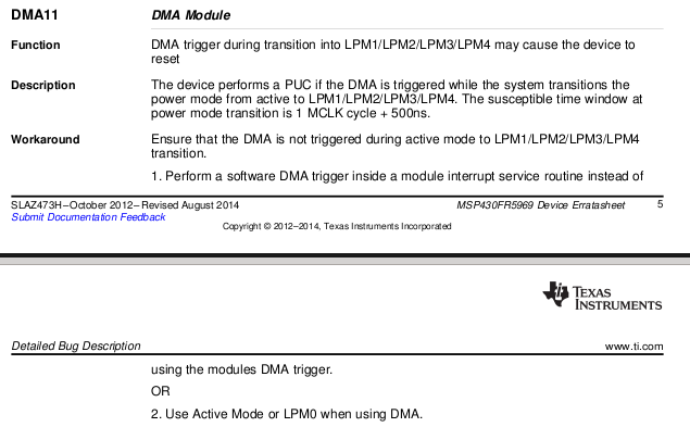
    The program uses DMA and enters LPM3. Therefore, maybe it is affected by the following MSP430FR5969 errata:

    Consider leaving running with zero wait states, but enter LPM0 instead of LPM3 and see if that stops the reset.

    [Errata DMA11 mentions a PUC reset rather than a ACCTEIFG reset, so may not be the cause]

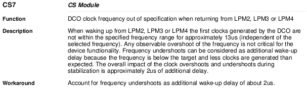
  • There is also errata CS7 related to waking up from LPM2, LPM3 or LPM4:

    While the description on CS7 says "Any observable overshoot of the frequency is not critical for the
    device functionality", it not clear how long a frequency overshoot has to occur before a FRAM wait state violation triggers a reset due to ACCTEIFG.

    Guess that so see if errata CS7 was the cause of the reset, would have to run with zero waits entering LPM3, but clocked off an external 8MHz crystal rather than the DCO.

  • More good stuff.  Thanks.  This has helped me think about different ways to approach my problem.

    First, running with zero wait states with LPM0 does seem to stop the resets.  I thought it interesting that when running in LPM0 I DO have to manually kick start the DMA by writing the first byte to the UART Tx buffer.

    Second, I tried running with zero wait states with LPM3 but never exiting LPM3 (thinking I might be able to do everything inside the Timer A ISR).  Still resets.  So, I enter LPM3 and the only thing happening should be the ISR:

    void TIMER3_A1_ISR(void)
    {
    	unsigned int taxiv;
    
    	// clear the interrupt
    	taxiv = TA3IV;
    
    	// do this the first time only
    	if(gDmaEnabled == 0)
    	{
    		// enable source DMA
    		DMA_enableTransfers(DMA_CHANNEL_0);
    
    		// kick off dma by manually sending first byte, rest of transfers handled by DMA
    		EUSCI_A_UART_transmitData(EUSCI_A1_BASE, 0x99);
    
    		gDmaEnabled = 1;
    	}
    }
    

  • So far, I have two options:  1) Run with wait states and LPM3 or 2) run with zero wait states and LPM0.

  • Thanks for all the responses.  I believe the cause of the reset is described by the DMA11 errata.  I thought I would go ahead and wrap this thread up.  For those interested, here is a brief summary of my progress.  I will start a new thread on the power consumption in LPM1 and LPM0 since it has nothing to do with the reset.  Thanks again!

    I am still becoming familiar with the MSP430.  In my application, I need SMCLK which sourced by the DCO. I have come to understand that I cannot enter LPM3 anyway if SMCLK is requested.  If I request LPM1, LPM2, or LPM3 I measure the same power consumption (which makes sense because the actual mode is always LPM1, I think).  However, the power consumption in LPM0 (~200uA) is less than that observed in LPM1(~350uA).  I am not sure if that makes sense, and, from the documentation, it is not yet clear what the difference is between the two.

  • Warren Langley said:
    I thought it interesting that when running in LPM0 I DO have to manually kick start the DMA by writing the first byte to the UART Tx buffer.

    It may be interesting, but it shouldn't be unexpected. The DMA engine needs to see the transition on the TXIFG flag to signal a start to DMA. I.e. it does not look for the flag being "already active" - it looks for it "going active".

    If you've done any serious ASIC or FPGA design (and the MSP430 is really just a special kind of ASIC) you understand why.... the peripherals can run on different clock domains. The UART could be on a slow clock and the DMA on a fast clock. It could take multiple DMA clocks before the UART flag changed back to low. So typically the signal is pipelined and the values of the last two stages of the pipeline are compared to look for a rising edge. And that is your DMA trigger.

    Pendants: Note that this may not be exactly how the MSP430 triggers are wired, but it's correct enough for this discussion.

  • Thanks, Brian.  Understood.

    I probably should have been more clear, but what was interesting to me was that I have to manually kick start the DMA when running in LPM0 but not when running in LPM1.  All along, I expected to have to manually kick start the DMA.

  • DMA requires MCLK. And if MCLK is set to DCO, DMA requires the DCO. Which is off in LPM1 and needs to be switched on and to stabilize. This process, if performed often, takes more average current than simply staying in LPM0 only.

    Also, this stretches the time between DMA trigger and DMA execution by the DCO wakeup time. This changes the timing of code/DMA execution and might be the reason why you’ll need ‘kickstart’ DMA in LPM0 but not in LPM1. Probably some timing problem in your code design that creates a racing condition.

**Attention** This is a public forum