This thread has been locked.

If you have a related question, please click the "Ask a related question" button in the top right corner. The newly created question will be automatically linked to this question.

Timers and PWM - MSP430G2553

Other Parts Discussed in Thread: MSP430G2553, MSP430G2452

Hello, to start off I am having trouble understanding the Timer modules availaible on the MSP430G2553 (Launchpad). In my user's guide, it mentions Timer B but apparently that's not on the chip.

Aside from that, I am trying to generate PWM from a timer. I am using the first timer for a real time clock, and I want to use another Timer for PWM. Here's what I have so far:

//configure Auxilary clock to run at 1 MHz
BCSCTL1 |= DIVA_0;
BCSCTL3 |= XCAP_3;
// Timer A1 PWM
TA1CCTL0 = OUTMOD_7;            // TACCR1 reset/set
TA1CTL   = TASSEL_2 + MC_1;     // SMCLK, upmode
TA1CCR0  = 1000-1;        // PWM Period
TA1CCR1  = 100;            // TACCR1 PWM Duty Cycle
P2DIR   |= BIT1;
P2SEL   |= BIT1;

I actually got that PWM snippet from somewhere online. However it's not working at all. What could be the issue?

  • Hi Sufyan!

    The G2553 has no Timer B, that's right. But it has two Timer A with 3 CC registers each.

    Haven't tested it, but try using P1.2 as the PWM output, changing your code to

    P1DIR |= 0x04;
    P1SEL |= 0x04;
    TA1CCTL1 = OUTMOD_7;
    TA1CCR0 = (1000 - 1);
    TA1CCR1 = 100;
    TA1CTL = (TASSEL_2 | MC_1);

    Dennis

  • Thanks for responding.

    I tried that code but it still didn't work. Also, I'm a bit confused. Why did you use P1.2 when according to the datasheet that's for TA0.1. Aren't we using TA1?

    Thanks.

  • Hi Sufyan!

    You have successfully passed the test!

    Of course you are absolutely right! This one belongs to TimerA0, sorry for that. But your BIT1 does also :-)

    So have you tried P2.1 / P2.2?

    Dennis

    Edit: Sorry again, your BIT1 was correct as you set it to P2 - shame on me.

  • Ok so after looking around for a while at the user's guide, datasheet, and online, I have decided that I don't understand this Timer module at all.

    From my understanding, there's TimerA0 and TimerA1. But online people are referring to both timers using the same registers, like this code:

    TACTL = TASSEL_1 + MC_1 + TACLR;
    CCR0 = 1000-1; // PWM Period
    CCTL1 = OUTMOD_7;// Reset/set
    CCR1 = 200-1; // 50% Duty cycle

    This code does not indicate if TimerA0 or TimerA1 is being used.

    My specific problem is that I am already using TimerA0 for something else. I would like to use TimerA1 for PWM generation. But my outputs are not working at all. Looking at the datasheet I have no idea how to select the pins to output TimerA1.

    So assuming I have programmed TimerA1 correctly to generate the required PWM, how can I specify which PIN I want to output to? Can you please be specific, the datasheet is confusing me very much. Because it mentions Timer1_A3.CCI0A and TIMER1_A3.TA1, and other confusing things which I don't understand.


    Thanks.

  • Hi Sufyan!

    You are right - the given names and abbreviations are (sorry TI) kind of horrible can be misleading in some cases. And they seem to change from one MCU to another.

    You have to look in the header file for the specific processor. Open the msp430g2553.h and search for TIMER, there you will find all of the definitions.

    If not exactly specified if TimerA0 or A1 it is TimerA0, so:

    • TACTL == TA0CTL
    • CCR0 == TACCR0 == TA0CCR0
    • CCR1 == TACCR1 == TA0CCR1
    • CCTL1 == TACCTL1 == TA0CCTL1

    There are two timer A modules with 3 CC registers each, that means:

    • TA0.0
    • TA0.1
    • TA0.2
    • TA1.0
    • TA1.1
    • TA1.2

    From each module TAx.1 and TAx.2 share one interrupt vector, TAx.0 has it's own one, so there are four interrupt-vectors:

    // Timer 0 A0 interrupt service routine
    #pragma vector = TIMER0_A0_VECTOR
    __interrupt void Timer0_A0_ISR( void )
    {
      ... // TA0CCR0
    }


    // Timer 0 A1 interrupt service routine
    #pragma vector = TIMER0_A1_VECTOR
    __interrupt void Timer0_A1_ISR( void )
    {
      switch( TA0IV )
      {
        case 2: // TA0CCR1
        {
          break;
        }
    
        case 4: // TA0CCR2
        {
          break;
        }
    
        case 10: // Overflow - TA0IFG
        {
          break;
        }
      }
    }


    // Timer 1 A0 interrupt service routine
    #pragma vector = TIMER1_A0_VECTOR
    __interrupt void Timer1_A0_ISR( void )
    {
      ... // TA1CCR0
    }


    // Timer 1 A1 interrupt service routine
    #pragma vector = TIMER1_A1_VECTOR
    __interrupt void Timer1_A1_ISR( void )
    {
      switch( TA1IV )
      {
        case 2: // TA1CCR1
        {
          break;
        }
    
        case 4: // TA1CCR2
        {
          break;
        }
    
        case 10: // Overflow - TA1IFG
        {
          break;
        }
      }
    }

    As you can see, even the ISR-vector-names are a little bit confusing...I know that you are not using the ISRs, but I explain it anyway.

    Each module has one CTL-register to set the basic operation of the module, so there are:

    • TA0CTL
    • TA1CTL

    With these registers you set one module for counting up/down/etc. and the input divider and the clock source. This gives you the possibility to source both modules from different clocks, like Timer A0 from an LFXT for counting seconds or anything else and the other one to SMCLK for example to do any other thing.

    Now there are the capture-compare-registers, three for TimerA0 and three for TimerA1:

    • TA0CCR0
    • TA0CCR1
    • TA0CCR2
    • TA1CCR0
    • TA1CCR1
    • TA1CCR2

    and the control-registers for the capture-compare-modes, again three for every module:

    • TA0CCTL0
    • TA0CCTL1
    • TA0CCTL2
    • TA1CCTL0
    • TA1CCTL1
    • TA1CCTL2

    The CCRx-registers set the timer-value at which the event takes place. These are 16-bit-registers, so the value can be an integer between 0 and 65535. The CCTLx-registers set the operating mode of each modules channel. For example you can set the CCIE-bit to enter the corresponding ISR and do some stuff if the TA0R-timer-value (for module TA0) or the TA1R-timer-value (for module TA1) matches the preset value in CCRx.

    So you can have six independent events. For example sourcing TA0 from LFXT 32k768-crystal, setting TA0CCR1 to 32768 in continous mode and enable the CCIE in TA0CCTL1. Add 32768 to TA1CCR1 in the ISR. This will result in having an interrupt every second.

    As you can see there is also the overflow interrupt which kicks in if the TAIE bit is set in TA0CTL or TA1CTL and the TAR-registers flow over. This overflow also shares the interrupt-vector with CCR1 and CCR2.

    You can now use the ISRs to set and reset a specific port-pin, but this needs code and execution-time. The MSP has the ability to do this completely in hardware, by setting the OUTMOD, as you already tried to do. In the datasheet you can see, which pin is associated to which timer. This is ideal for generating a PWM.

    For the MSP430G2553 (PW20/N20) this is:

    • P1.1 - TA0.0 - TA0CCR0
    • P1.2 - TA0.1 - TA0CCR1
    • P1.5 - TA0.0 - TA0CCR0
    • P1.6 - TA0.1 - TA0CCR1
    • P2.0 - TA1.0 - TA1CCR0
    • P2.1 - TA1.1 - TA1CCR1
    • P2.2 - TA1.1 - TA1CCR1
    • P2.3 - TA1.0 - TA1CCR0
    • P2.4 - TA1.2 - TA1CCR2
    • P2.5 - TA1.2 - TA1CCR2

    Taking OUTMOD_7 in timer UP-mode for a PWM does the following: Set the pin high if counting to CCR0 and reset it to low when reaching CCR1 (could be CCR2, too, of course). So CCR0 sets your period and CCR1 sets the duty-cycle of the PWM-signal. As you can see, CCR0 should be greater than CCR1. And the other thing you can see: CCR0 sets the period for both CCR1 and CCR2. This is why CCR0 always is something "special" and even has it's own ISR.

    Now you are free to chose which pin you want to use. Let's take TA1 (second timer module) and from this module we take CCR1 for setting our duty-cycle. We can now choose between P2.1 and P2.2 - so let's take P2.1 on pin 9 of the MCU. This pin is set to GPIO-function and as an input after startup. We want it to be linked to the timer-module, so we will look at the datasheet and find on page 51, that the P2.1 is connected to the timer by setting the following:

    P2DIR  |=  0x02; // Set P2.1 to output-direction
    P2SEL  |=  0x02; // Set selection register 1 for timer-function
    P2SEL2 &= ~0x02; // Clear selection register 2 for timer-function (not needed, as it is 0 after startup)

    Now we have to set up the timer. Let's source it from SMCLK with the calibrated 1MHz DCO-clock. We set:

    TA1CCTL1 = OUTMOD_7;          // Reset/set
    TA1CCR0  = 20000;             // Period
    TA1CCR1  = 1500;              // Duty-cycle
    TA1CTL   = (TASSEL_2 | MC_1); // SMCLK, timer in up-mode

    This will give us a signal with a period of about 20ms with a duty-cycle of 1.5ms - hey perfect to drive a RC-servo.

    Now let's make a program from that:

    #include "msp430g2553.h"
    
    void main( void )
    {
      WDTCTL    = WDTPW | WDTHOLD;   // Stop watchdog timer
    
      BCSCTL1   = CALBC1_1MHZ;       // Set DCO range
      DCOCTL    = CALDCO_1MHZ;       // Set DCO step and modulation
    
      P2DIR    |=  0x02;             // Set P2.1 to output-direction
      P2SEL    |=  0x02;             // Set selection register 1 for timer-function
      P2SEL2   &= ~0x02;             // Clear selection register 2 for timer-function (not needed, as it is 0 after startup)
    
      TA1CCTL1  = OUTMOD_7;          // Reset/set
      TA1CCR0   = 20000;             // Period
      TA1CCR1   = 1500;              // Duty-cycle
      TA1CTL    = (TASSEL_2 | MC_1); // SMCLK, timer in up-mode
    
      while( 1 )                     // Endless-loop (main-program)
      {
                                     // Do nothing, hardware-based PWM
      }
    }

    Unfortunately I haven't got a MSP430G2553 at the moment - so I haven't tested it. Correct me if something is wrong. But I hope that helps a little bit, at least to understand all these names and abbreviations. Always have a look at the MCU-specific header-file :-)

    Dennis

  • Hi, it's me again!

    #FreeSampleCode

    I've found a MSP430G2452 and tested the code. This processor only has one TimerA3, so I use TA0.1 on P1.2 for my PWM-output. This is the code:

    #include "msp430g2452.h"
    
    void main( void )
    {
      WDTCTL    = WDTPW | WDTHOLD;   // Stop watchdog timer
    
      BCSCTL1   = CALBC1_1MHZ;       // Set DCO range
      DCOCTL    = CALDCO_1MHZ;       // Set DCO step and modulation
    
      P1DIR    |=  0x04;             // Set P1.2 to output-direction
      P1SEL    |=  0x04;             // Set selection register 1 for timer-function
      P1SEL2   &= ~0x04;             // Clear selection register 2 for timer-function (not needed, as it is 0 after startup)
    
      TA0CCTL1  = OUTMOD_7;          // Reset/set
      TA0CCR0   = 20000;             // Period
      TA0CCR1   = 1500;              // Duty-cycle
      TA0CTL    = (TASSEL_2 | MC_1); // SMCLK, timer in up-mode
      
      while( 1 )                     // Endless-loop (main-program)
      {
                                     // Do nothing, hardware-based PWM
      }
    }

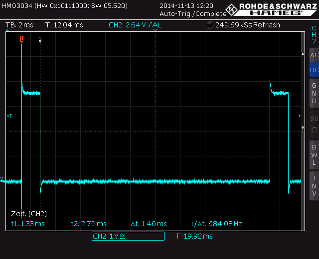
    And this is the result:

    As you can see there is a period of 19.92ms with a duty-cycle of 1.46ms - good enough.

    Dennis

  • Dennis Eichmann said:
    You are right - the given names and abbreviations are (sorry TI) kind of horrible in some cases. And they seem to change from one MCU to another.

    It's quite simple if you know the history.

    When there once was only one timer, it was TimerA. And TA was omitted from the register names (CCRx, CCTLx).

    Then there was TimerB (but still only one TimerA per device), so the naming changed to TACCRx.
    Finally, there appeared devices with more than one TimerA, so the names changed to TAyCCRx.
    So if there is no timer letter or not timer count, it refers to TimerA0.

    The interrupt vectors have undergone a similar change:
    Originally, there was TIMER_A0_VECTOR and TIMER_A1_VECTOR, being vector #0 and #1 for TimerA0.
    With introduction of the presence of a Timer1, this has changed to TIMER1_A0_VECTOR and TIMER1_A1_VECTOR for vector #0 and #1 of TimerA1. Maybe not the best choice. TIMERA1_0_VECTOR would have been clearer. Or TIMERA1_VECTOR0.

  • Thank you so so much for such a detailed response. It finally worked and I understand the Timer module in quite a good depth now, I think.

    Also, from my original code there was a minor mistake which your code corrected.

    I had TA1CCTL0 instead of TA1CCTL1.

    I ended up making a function which allows me to select the frequency and duty cycle (within an operable range of course).

    Again thank you so much for the effort.

  • First of all thank you for such a nice and detailed explanation.!!

    "Now you are free to chose which pin you want to use. Let's take TA1 (second timer module) and from this module we take CCR1 for setting our duty-cycle. We can now choose between P2.1 and P2.2 "

    As you mentioned above that any pin can be selected for pwm operation, i have used BOTH the pins as OUTPUT.

    The reason is, i want to drive 4 MOSFET in an interleaved synchronous buck regulator and i am using 2 half bridge IRS2003 MOSFET driver.

    The MOSFET Driver is designed for such type of application where only one pwm input is required if we SHORT both HIN and LIN inputI.

    I.e. The internal circuit will take care of the two MOSFET not being ON together. 

    HIGH input TO HIN will output HIGH at HO

    HIGH input TO LIN will output LOW at LO with some dead time.

    NOW, PIN2.1 will be input to MOSFET DRIVER 1 and PIN2.2 will be input to MOSFET DRIVER 2, ensuring BOTH HIGH SIDE mosfet are ON simultaneously and BOTH LOW SIDE mosfet are OFF simulataneously thus ensuring interleaved synchronous buck operation.

    I have updated the pin configuration of the same code you have written.

    Can you please verify that my logic is correct and the code i have written should work....!!!

    #include "msp430g2553.h"
    
    void main( void )
    {
      WDTCTL    = WDTPW | WDTHOLD;   // Stop watchdog timer
    
      BCSCTL1   = CALBC1_1MHZ;       // Set DCO range
      DCOCTL    = CALDCO_1MHZ;       // Set DCO step and modulation
    
      P2DIR    |=  0x06;             // Set P2.1 and P2.2 as an output-direction
      P2SEL    |=  0x06;             // Set selection register 1 for timer-function
      P2SEL2   &= ~0x06;             // Clear selection register 2 for timer-function (not needed, as it is 0 after startup)
    
      TA1CCTL1  = OUTMOD_7;          // Reset/set
      TA1CCR0   = 20000;             // Period
      TA1CCR1   = 1500;              // Duty-cycle
      TA1CTL    = (TASSEL_2 | MC_1); // SMCLK, timer in up-mode
    
      while( 1 )                     // Endless-loop (main-program)
      {
                                     // Do nothing, hardware-based PWM
      }
    }

    Thank you in advance..!
  • I am going to try the same thing like you but using two IR 2104 MOSFET Driver for a H-brigde construction.
    Like usual for H-bridge I'd linke to change the direction of the motor rotation.

    For example right turn: T4 on permanently // T1&T3 PWM signal in
    For example right left: T3 on permanently // T2&T4 PWM signal in

    So I do need two pins supporting the same pwm duty_cycle range but have to switch these pins for motor-rotation-change and set the other pin low. How to do that with pushing a button like "rotation change"?

    Please help!
    Thanks a lot!

  • The PWM signals on P2.1 and P2.2 are exactly the same. I think you are going to burn your bridge.
  • I haven't post a code so far. Port 2 is in use for a lcd so i only can only choose Port1 for PWM signal out. As i have tried to describe: i need to change the Bit on Port1 for motor rotaion change. If there would be a small delay in between its not going to happen burning the bridge.
  • In your reply to AMIT, you said "I am going to try the same thing like you .."

    Well, in AMIT's code, P2.1 and P2.2 have identical waveform. Thus all 4 arms of your H bridge will be turned on at the same time.

    It is possible to generate two different PWMs on two different Port 2 pins.
    But for the 20-pin package, it is not possible to generate two different PWM signals on two different Port1 pins.

    See MSP430G2553 Data-sheet Table 12. Timer0_A3 Signal Connections and Table 13. Timer1_A3 Signal Connections.

    (Edited)

**Attention** This is a public forum