This thread has been locked.

If you have a related question, please click the "Ask a related question" button in the top right corner. The newly created question will be automatically linked to this question.

MSP430FR5969 using a timer to trigger ADC12

Other Parts Discussed in Thread: MSP430FR5969

Hi, ive been trying to trigger an adc12 repeat sequence of channels conversion from timer A1 (because these are the pin outputs i can verify on the launchpad board). The timer runs of an 32 kHz external crystal oscillator and i desire the ADC to sample at 8 kHz. I've looked at several forum posts but none have answered my questions and the data sheet/ user guide is vague on the relationships between the timer and ADC12 trigger.

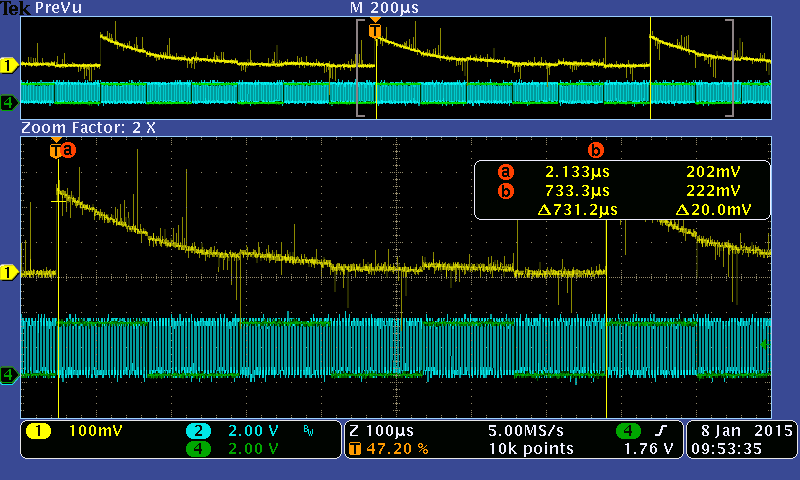
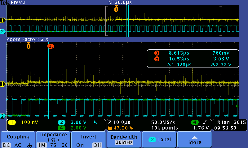
I set P3.6 to toggle to view timings on an oscilloscope. The PWM triggers correctly however the ADC triggers at around 600 kHz with the MCLK (still active. I have tried the setup from triggering a timer interrupt and starting the ADC via a software however I cannot get this to work.

Please find my code attached and any help would be very much appreciated.

#include <msp430.h>

int main(void)
{
  WDTCTL = WDTPW | WDTHOLD;                 // Stop WDT

  // GPIO Setup  // Configure GPIO for timer, set all registers to output to reduce current leaks
  P1OUT &= ~BIT0;                           // Clear LED to start
  P1DIR |= 0xFF;                            // Set P1.0/LED to output
  P4DIR |= 0xFF;
  P3DIR |= 0xFF;
  P2DIR |= 0xFF;
  PJDIR |= 0xFF;


  P1OUT &= ~BIT0;                           // Clear LED to start
  P1DIR |= BIT0;                            // Set P1.0/LED to output
  P1SEL1 |= BIT1;                           // Configure P1.1 for ADC
  P1SEL0 |= BIT1;

  P3OUT |= BIT6;

  P1SEL0 |= BIT2;                    		// P1.2 options select

  //configure gpio for adc
  P1SEL1 |= BIT3 | BIT4 | BIT5;             // Configure ADC inputs A1, A2 and A3
  P1SEL0 |= BIT3 | BIT4 | BIT5;

  //enable XTLFO gpio
    PJSEL0 |= BIT4 | BIT5;

  // Disable the GPIO power-on default high-impedance mode to activate
  // previously configured port settings
  PM5CTL0 &= ~LOCKLPM5;

  FRCTL0 = FRCTLPW | NWAITS0;

  // Setup XT1 crystal.Set the Master and SM (16 MHz) and ACLK (XT1)
  CSCTL0_H = CSKEY >> 8;                    // Unlock CS registers
  CSCTL1 = DCORSEL | DCOFSEL_4;                   // Set DCO to 16MHz
  CSCTL2 = SELA__LFXTCLK | SELS__DCOCLK | SELM__DCOCLK; // set ACLK = XT1; MCLK = SMCLK = DCO
  CSCTL3 = DIVA__1 | DIVS__1 | DIVM__1;     // Set all dividers
  CSCTL4 &= ~LFXTOFF;
  //Wait for the oscilator to settle
  do
  {
    CSCTL5 &= ~LFXTOFFG;                    // Clear XT1 fault flag
    SFRIFG1 &= ~OFIFG;
  }while (SFRIFG1&OFIFG);                   // Test oscillator fault flag
  CSCTL0_H = 0;                             // Lock CS registers

  ADC12CTL0 = ADC12MSC | ADC12ON;       // Sampling time, ADC12 on
  ADC12CTL1 = ADC12CONSEQ1 | ADC12CONSEQ0 | ADC12SHP | ADC12SHS_4;  // repeat sequence of channels, triggers from TA1
  ADC12CTL2 |= ADC12RES_2;                  // 12-bit conversion results

  ADC12MCTL0 |= ADC12INCH_3;			     // Channel2 ADC input select; Vref=AVCC
  ADC12MCTL1 |= ADC12INCH_4;			     // Channel2 ADC input select; Vref=AVCC
  ADC12MCTL2 |= ADC12INCH_5 | ADC12EOS;	     // Channel2 ADC input select; Vref=AVCC

  ADC12IER0 |=  ADC12IE2;

  ADC12CTL0 |= ADC12ENC;

  //configure timer A1 for puslse width toggle option
  TA1CCTL1 = OUTMOD_4;                      // CCR1 toggle and interrupt enabled
  TA1CCR0 = 4-1;
  TA1CCR1 = 0;

  TA1CTL = TASSEL__ACLK | MC__UP | TACLR; // ACLK, up countmode, clear TAR

  __bis_SR_register(LPM3_bits | GIE);     // LPM0, ADC12_ISR will force exit
}

#if defined(__TI_COMPILER_VERSION__) || defined(__IAR_SYSTEMS_ICC__)
#pragma vector = ADC12_VECTOR
__interrupt void ADC12_ISR(void)
#elif defined(__GNUC__)
void __attribute__ ((interrupt(ADC12_VECTOR))) ADC12_ISR (void)
#else
#error Compiler not supported!
#endif
{
  switch(__even_in_range(ADC12IV, ADC12IV_ADC12RDYIFG))
  {
    case ADC12IV_ADC12IFG2:
    	P3OUT ^= BIT6;
    	break;        // Vector 16:  ADC12MEM2
    default: break;
  }
}

  • Hi Sam,

    I think the problem might be that you have set the ADC12MSC bit. Looking in the user's guide www.ti.com/lit/pdf/slau367 section 25.2.8.5 on p. 663:

    "When ADC12MSC = 1, CONSEQx > 0, and the sample timer is used, the first rising edge of the SHI signal triggers the first conversion. Successive conversions are triggered automatically as soon as the prior conversion is completed (if the ADC local reference buffer is used, ADC12VRSEL= 0001, 0011, 0101, 0111, 1001, 1011, 1101, or 1111, there is one clock cycle before the successive conversion is triggered). Additional rising edges on SHI are ignored until the sequence is completed in the single-sequence mode, or until the ADC12ENC bit is toggled in repeat single-channel or repeated-sequence modes."

    So basically if you set this bit the ADC is going to sample as fast as it can, even if the timer hasn't triggered it again yet - it will start a new conversion immediately when the previous one is done. Maybe try also looking at the MSP430FR5969 example msp430fr59xx_adc12_11.c, (in TI Resource Explorer in CCS, or here www.ti.com/lit/zip/slac536 ) as it shows doing a timer triggered repeated single channel. You would then just extend to repeated sequence and using TA1.1 instead of TA0.1.

    Hope this helps point you in the right direction.

    Regards,

    Katie

  • Thanks, that was it!
  • sorry that wasn't the right answer as I said before, I was looking at the wrong output pin. The debugging seems to be strage as the first time i run the program under debug stage nothing happens, but I I pause and restart I see waveforms on my Osc scope (pin setting and ADC sampling). Below are the wave forms I see.

    Yellow = ADC input A3, Blue is the toggling of pin 3.6 and Green is the output of the PWM for the timer (128 Hz toggle) 

    The top capture shows the ADC seems to sample ~ 1.3 kHz (however there are glitches at 128 Hz in the waveform) and the bttom capture shows the toggling of pin3.6 at 530 kHz. Wehn running the scope as well the trigger is based on the PWM of the timer (green), but the ADC input (yellow) us not synchronous with this and shows a lot of jitter. There are only two things I can think which might be problamiatic. It either does not work in LPM3 which isnt suggested in the data sheet or when I tested it in active mode (using an infinite while loop) or a problem with the trigger. The data sheet (p66) describes the trigger as the TA1 CCR1 output, however I have no idea what this means as the CCR1 is a passive register, does it mean it compare the timer count to that of the value stored in CCR1, or that you cant use toggle mode as CCR1 is not taken into account in the PWM? 

  • Hi Sam,

    Sorry to hear of your ongoing difficulties. I took another look into this and tried the code a bit myself, as well as comparing it to the code example msp430fr59xx_adc12_11.c that shows doing a timer triggered ADC. What I've found is that I believe you are actually running into one of the errata on the FR5969 device. In the errata document here: www.ti.com/lit/pdf/slaz473 See ADC41:

    "ADC41 ADC12_B Module

    Function ADC conversion only triggers when sourced from TA0 and TA3 in LPM3/LPM4

    Description If the ADC clock is sourced from ADC12OSC (ADC12CTL1.ADC12SSELx = ADC12OSC), the reference module is not used (REFCTL0.REFON = 0), and the device is in LPM3/LPM4 mode, ADC conversion cannot be triggered when using Timer TB0, TA1 and TA2 (ADC12CTL1.ADC12SHSx).

    Workaround 1. Use Timer TA0 or TA3 to trigger ADC conversion in LPM3/LPM4 mode

    OR

    2. Configure ADC clock to be sourced from ACLK (ADC12CTL1.ADC12SSELx = ACLK).

    OR

    3. Use Active/LPM0/LPM1/LPM2 mode

    OR

    4. Use the internal voltage reference (REFCTL0.REFON = 1)"

    So I would recommend either using TA0.1 or TA3.1 instead of TA1.1, or using one of the workarounds like using the internal reference or a different low power mode.

    Regards,

    Katie

  • Sam Moreland said:
    The data sheet (p66) describes the trigger as the TA1 CCR1 output, however I have no idea what this means as the CCR1 is a passive register, does it mean it compare the timer count to that of the value stored in CCR1, or that you cant use toggle mode as CCR1 is not taken into account in the PWM? 

    I also meant to explain what is meant by TA1 CCR1 output. Look at the user's guide for this device www.ti.com/lit/pdf/slau367  Figure 16-1, the Timer_A Block Diagram. If you look at the CCR6 block, you'll see they have "OUT6 Signal" labeled. There is one of these blocks and one of these output signals for every CCRx register in the timer module. This OUTx signal is what is meant by the TA1 CCR1 output - it is the PWM that comes out of the module.

    The datasheet table you mentioned is telling you that, in addition to having the potential to output this signal externally on the pins by setting the PxSELx bits, the signal is also connected internally to the ADC and can be selected to be used as the trigger signal by setting the ADC12SHSx bits. You can see this in the same user's guide www.ti.com/lit/pdf/slau367 in the ADC12_B block diagram on Figure 25-1. The right side of the figure you will see "trigger sources" and the ADC12SHSx bits used as the select lines for a mux to select the trigger source signal. The TA1 CCR1 output signal is connected in the part internally as one of these trigger sources.

    Regards,

    Katie

**Attention** This is a public forum