This thread has been locked.

If you have a related question, please click the "Ask a related question" button in the top right corner. The newly created question will be automatically linked to this question.

MSP430 SPI slave clock specification

Other Parts Discussed in Thread: MSP430F5132, ADS7946, MSP430FR5969

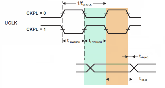
I am planning to use MSP430F5132 in SPI slave mode. What are the specifications for the clock? In the datasheet (SLAS619M, pages 33-34), low and high times are marked as t low/high and period is marked as 1/f UCXCLK, but I can't find any values for these parameters.  I would like to use a 25 MHz clock. If it is possible to step up the clock to 40 MHz, it would be nice. I will not use SOMI data at all - it will not be connected.

  • Hi Kurt,

    To calculate the maximum frequency for SPI on MSP430, there is an equation: (1) fUCxCLK = 1/2tLO/HI with tLO/HI max(tVALID,MO(Master) + tSU,SI(USCI), tSU,MI(Master) + tVALID,SO(USCI)). For the master's parameters tSU,MI(Master) and tVALID,MO(Master), see the SPI parameters of the attached master. This equation is usually included as a footnote on the SPI specs of the datasheet (for example see www.ti.com/lit/gpn/msp430f5529 footnote (1) on p. 67) but it seems to be missing from the F5132 datasheet - I've filed this to be fixed so as to prevent further confusion in the future.

    This post discusses a similar situation: http://e2e.ti.com/support/microcontrollers/msp430/f/166/p/203168/721572#721572 In that post he calculates the value for using 2 MSP430s, one as master and one as slave, as being about 7MHz. You need to take the Master timings in the equation from the master device that will be communicating with the MSP430. If you are unsure of what some of the timings are in the equation (like tVALID,MO(Master)) you can find in the datasheet for your device www.ti.com/lit/gpn/msp430f5132 there are some diagrams Figure 5-23 through 5-26 that show what timings on the waveforms are meant by this notation, as the notation on your master device datasheet may be a little bit different.

    This is not going to come out anywhere near 25MHz. As Jason pointed out for the 2 MSP430 case it is only about 7MHz - I don't think any of our MSP430 devices, even with eUSCI module instead of USCI, will get you near 25MHz. Even if you could clock the module reliably that fast where all the setup/hold timings etc worked in the equation I mentioned above, the max system frequency of the MSP430F5132 device is still only 25MHz. So even if you could clock in/out data that fast on the module, it is unlikely your code would be able to keep up in order to keep the transmit/receive registers loaded/read with only 8 CPU cycles per byte received/sent (since running at 25MHz and tx/rx at 25Mbps), or be able to do anything useful with the information at all in that amount of time.

    What is the purpose in this application of having such fast data speeds with the MSP430 as the slave?

    Regards,

    Katie

  • I saw that footnote in other MSP430 datasheets. However, it doesn't make sense in my application since I don't plan to use output from the SOMI pin.

    What I want to do is to connect an ADC (ADS7946) that can deliver up to 40 mbit/s data to SIMO and USCICLK. I don't intend to use data coming out from the SOMI pin on the MSP430. The incoming data can be transferred to internal RAM with DMA. With 25 MHz clock, I will get 2 bytes back to back every 800 nanosecond, which will be 2.5 Mbyte/second. The DMA should be able to handle that. This will repeat during a short time. After that, software in the MSP430 makes calculations on received data.

    As I understand it, the USCI will output content of TXBUF on the SOMI pin. But if I don't care what it is, do I have to load the TXBUF?

    The specs on setup and hold times is very good. I don't see any problem with this, but I may be missing something.

    Best regards

    Kurt
  • The proper specification for input clock in slave mode should be minimum low & high time, maybe together with the note you mention that are on other MSP430 datasheets. If I use the note in my situation I would get t valid,MO max = 9 ns (@3V) and t setup SI USCI min = 2 ns@3V resulting in t low/high = 11 ns and a possible CLK frequency of 40 MHz (assuming fall/rise time of 1.5 ns). I can imagine other devices that produces data faster which would lead to even faster clocks if it was only the note that determined minimum pulse width.
  • Hi Kurt,

    Thanks for the additional information about your application and it sounds like your case is a little bit different from the typical one - this makes clearer what you are trying to do and what will apply in your particular case. 

    However, I was looking at the ADS7946 datasheet and I see that it labels SCLK and CS (chip select) as being digital inputs - so I think the ADS7946 has to be the SPI slave instead of the SPI master. I believe you must supply SCLK to it from the master for the ADS7946 to operate, and you'll have to select the ADS device with a GPIO from the MSP on the CS chip select line of the ADS device for it to convert and output data.This means the MSP430 will be the master, and that will make your code easier and make it easier to make sure the MSP can always keep up, as you will supply and control SCLK frequency from the MSP which also will determine your ADC frequency - the MSP430 will also get to control requesting data to be output from the ADS device because it has the CS pin, so it will be able to de-select the device if the MSP is not ready to take another reading/receive more data yet. This is also the more typical usage for the microcontroller to be the master and the ADC to be the slave.  

    So I actually think you're going to have to use the MSP430 as the master in the equations instead of the slave as we discussed above, but you still have the benefit of the fact that the ADC never receives any data from the MSP430, it only sends data out back to the MSP - so you can ignore any MOSI specs and focus only on timings for MISO. Calculating this, I think you have tSU,MI = 25ns from MSP430 datasheet, tVALID,SO = 9ns (@3V) from ADS datasheet. The other part of the equation (tVALID,MO and tSU,SI are for Master-Out-Slave-In MOSI so you can ignore in this case since you'll never do that). So you get tLo/Hi >= 9 + 25 ns = 34ns. 1/(2tLo/Hi) = ~14.7MHz.

    Regards,

    Katie

  • Hi Katie,

    If I use MSP430 Master mode, I have to both write TX reg even if I don't use the data and read RX reg. My plan is to supply clock to both ADS7946 and MSP430 from an external source and run MSP430 as slave with input data only and use one DMA channel to transfer received data to internal RAM. This approach will use minimal resources and will also be very fast.

    As I said earlier, there has to be a minimum low/high time for SPI clock in slave mode. Could you please try to find that specification? I would also like to know if there is any potential problem that TX reg is not loaded in this mode.

    Best regards

    Kurt Mirdell

  • Hi Kurt,
     
    The calculation that you did before is correct for slave mode if you are not sending anything back to the master. So I think you've got that calculated and the limitation then is just going to be your DMA/software handling. There also should be no problem with not loading TXBUF if you aren't ever sending anything to the other device, just receiving. Best of luck with your application!
    Regards,
    Katie

  • Hi Katie,
    I am sorry, but since I don't get any clear specification on minimum SPI clock times low/high, I feel reluctant to use the MSP430 all together. I will have to look for other solutions. Most other manufacturers specify this clearly, however often with rather low speeds. With TI's spec, I feel unsure if it will work reliable on any unit.
  • Kurt,

    I am sorry to hear of your frustration and I'm very sorry that the tLo/Hi equation was missing from this particular datasheet. Instead of just giving a flat number for tLO/HI we specify it in terms of the valid, setup, and hold times for master mode and slave mode on the MSP430, and these are all specified with worst case specs that are guaranteed across all device variation and over recommended ranges of supply voltage and temperature. The timings are also diagrammed to help you understand our notation if it differs from other devices you are used to.

    Then you simply use the equation (also normally in the datasheet) to plug in the timings from the device that is on the other side of your communication to find the required tLo/Hi - this is an attempt to make the spec actually more specific and give you more information. We do not simply specify a flat number for tLo/Hi because this depends not only on the MSP timings, but also on the device that you are trying to communicate with and its timings - this is why we provide you with the equation telling you to take the maximum time of the two sides of the communication (SIMO or SOMI) to be your worst case.

    Including the specs from your other side of the communication helps make sure that this spec is as accurate as possible for a user's particular use case - as you've seen your use case is different from the standard one, and this tLO/HI equation then means you will plug in values for your use case. Since you have no communication in one of the directions (data from the MSP to the ADC), so you can just plug in 0 for those timings as it is a don't care for you, then take the worst case spec from the MSP and ADC datasheets for the other timings. This lets the spec be more specific than if it simply stated a flat tLO/HI time because that would not distinguish between the two directions of the communication where one does not matter in your case, or account for the timing of your other device.

    As far as the footnote with the equation being missing from this particular datasheet:

    I have filed a request already for this to be updated but it may take a little bit of time to make it to our website. However I have checked with our design and this equation does apply to this device (and all of our devices with USCI SPI). This is what it will look like when updated:

    on the slave mode specs:

    "(1) fUCxCLK = 1/2tLO/HI with tLO/HI ≥ max(tVALID,MO(Master) + tSU,SI(USCI), tSU,MI(Master) + tVALID,SO(USCI)).

    For the master's parameters tSU,MI(Master) and tVALID,MO(Master), see the SPI parameters of the attached master."

    on the master mode specs:

    "

    (1) fUCxCLK = 1/2tLO/HI with tLO/HI max(tVALID,MO(USCI) + tSU,SI(Slave), tSU,MI(USCI) + tVALID,SO(Slave)).

    For the slave's parameters tSU,SI(Slave) and tVALID,SO(Slave) see the SPI parameters of the attached slave."

    Again, I am sorry for your experience, and I hope that the spec is now clear to you.

    Regards,

    Katie

  • Hi Katie,

    The TI spec is good in one way because it focus on the other connected device, which other manufacturers don't do. However, the TI spec is seriously flawed because it doesn't give minimum values for t low and t high. With a device that delivers data with very short delay, TI's incomplete specs says that it would be possible with data rates of more than 100 MHz, which is not likely.

    My construction will be used in a commercial product. If I test this on one device and it works, how do I know that it will work on all devices? Maybe you are doing a minor change that affects this, and suddenly nothing works. I am used to do things according to specs.

    In my opinion, TI need to add a specification for minimum t low and/or t high when MSP430 is used as a SPI slave. It is also important to specify if any of the system clocks are a limiting factor.

    Best regards

    Kurt Mirdell

  • Please do a sanity check. The said hold times are because of propagation delays between clock and data lines. This is a requirement that is independent of the clock speed. They do not specify a maximum clock frequency for the complete circuitry.
    There is no port pin maximum frequency specified explicitly, but the datasheet specifies a minimum trigger pulse duration of 20ns. It is sane to assume that this means that the port logic is specified for a maximum clock frequency of 25MHz (50% DC).
    Also, a DMA transfer, while the CPU is still running, will take 4 MCLK cycles, which is 50% of the memory bus time. On higher speeds, you wouldn't have any CPU time left to do anything with your data.
    Also, do you need this speed? You said you plan to provide the clock externally. Fine. But then it is you who defines the speed. It is no necessity of an external master.
    With 25MHz, even the MSP with the biggest ram will be filled within 21ms, with no chance to do any realtime processing of an input stream. Is there a sane reason why you want to do it faster?
    If not, then the whole discussion is pointless. But if there is, then you should know how fast _exactly_ the transfer _has_ to be, and the question is not 'how fast can the MSP do' but rather 'can the MSP do it exactly that fast'. Which is way more easily to answer.
  • If you read what I have written, I am complaining about a statement from a TI employe that tells me that I could run use a SPI clock in excess of 100 MHz. I don't believe that.

    My plan is to receive data at high speed in a short burst, maybe 50 samples. After that burst, I will have plenty of time to process the data.

    I was asking for a clarification of the data sheet. I was asking for the maximum frequency of the spi slave clock, but did not get that.

    There is a specification for maximum clock output frequency on a pin for the MSP430.

    You can of course assume anything. But if you want to do electronic constructions that works, you are much better of if you don't assume, but instead are using specifications.

    As I have described, I intend to use an ADC that could run with up to 40 MHz clock. Higher frequency results in more measurements during the same time, which gives better accuracy due to oversampling. For that reason, the exact question is "how fast can the MCU do it". If the MCU can't do it at 40 MHz, I can lower the speed to a rate that works. But then I won't use the ADC's potential.

    Result of this is that I will not use the MSP430 for my application. I have found an other MCU.
  • This is only loosely related to the original question, but I think the formula for maximum frequency given in the footnote is incomplete.

    fUCxCLK = 1/2tLO/HI
    tLO/HI ≥ max(tVALID,MO(Master) + tSU,SI(Slave), tSU,MI(Master) + tVALID,SO(Slave))

    It covers both SIMO and SOMI, but only guarantees that the clock is slow enough to meet the timing constraints that apply to one half of the clock cycle. It ensures that each bit (in either direction) is transmitted early enough that the receiver will not sample it before it has settled. The formula assumes the other half of the clock cycle doesn't need to be longer than this half, which is not always the case.

    The following diagram shows the (tVALID,MO(Master) + tSU,SI(Slave)) part of the formula (ie the first parameter to max):

    Note that the second parameter to max refers to the same half-cycle of the SPI clock, but for transmission in the opposite direction (slave to master).

    The other half of the clock cycle looks like this (again, showing only transmission from master to slave):

    This represents the requirement that the value on the line be stable until after the receiving end has finished sampling it. If tHD,MO is positive that means the line will stay valid beyond the clock edge that triggers output change, giving the receiver more time to sample. This parameter may be negative (ie the output changes before the clock edge).

    The formula based on this half of the cycle would be:

    fUCxCLK = 1/2tLO/HI
    tLO/HI ≥ max(tHD,MI(Master) - tHD,SO(Slave), tHD,SI(Slave) - tHD,MO(Master))

    And combining the two gives:

    fUCxCLK = 1/2tLO/HI
    tLO/HI ≥ max(tVALID,MO(Master) + tSU,SI(Slave), tSU,MI(Master) + tVALID,SO(Slave), tHD,MI(Master) - tHD,SO(Slave), tHD,SI(Slave) - tHD,MO(Master))

    Or alternatively:

    fUCxCLK = 1/2max(tA, tB)
    tA ≥ max(tVALID,MO(Master) + tSU,SI(Slave), tSU,MI(Master) + tVALID,SO(Slave))
    tB ≥ max(tHD,MI(Master) - tHD,SO(Slave), tHD,SI(Slave) - tHD,MO(Master))

    For an example of where this matters, looks at the datasheets for the MSP430FR5969 and Sharp 96x96 memory LCD display. The display doesn't transmit anything, so based on the first formula tLO/HI would be 10 + 380ns. That gives a maximum frequency of 1.28MHz. With the second formula tLO/HI works out as 440 - 0ns, so the maximum frequency that satisfies the hold time requirement is 1.14MHz.

    (NB: I've ignored the signal rise times, but I think they just add 50ns to both half-cycle calculations in the worst case)

  • Kurt Mirdell said:
    You can of course assume anything.

    You can. But I wasn't talking about plain guessing. I was talking about using the available information.
    If a device is rectangular and its with and height is given, there is no point in giving the length of the diagonal or its circumference too.

    You can fill the datasheet with another 100 pages of superfluous information. And surely some of it will be useful for someone sometimes.

    Kurt Mirdell said:
    I am complaining about a statement from a TI employe that tells me that I could run use a SPI clock in excess of 100 MHz. I don't believe that.


    Well, if not limited by any other parameter given in the datasheet, you need 2 MCLK cycles to transfer a byte from RXBUF to memory. With 25MHz maximum MCLK speed and 8 bit per byte, 100MHz SPI clock do not seem impossible. More would make no sense.

    However, the timing limitations for the IRQ detection logic seem to indicate that the CMOS gates aren't as fast.

    Kurt Mirdell said:
    if you want to do electronic constructions that works, you are much better of if you don't assume, but instead are using specifications.

    And if you want your work done and don't have the information you need, find it out yourself. Engineering is more than just clicking things together from predefined sheets.

    Kurt Mirdell said:
    I intend to use an ADC that could run with up to 40 MHz clock.

    Which doesn't mean it will output 5MB data per second. Unless it is a delta-sigma with continuous output bitstream.
    Kurt Mirdell said:
    Higher frequency results in more measurements during the same time, which gives better accuracy due to oversampling.
    Does it? Depends on several factors. Usually, what people call *oversampling' only results in smoothing the results (averaging), not in increased accuracy. Like zipping a JPEG won't reduce the size.

    Kurt Mirdell said:
    Result of this is that I will not use the MSP430 for my application. I have found an other MCU.

    Use the right tool for the job. If you don't think the MSP will suit your needs, then don't use it.
    Personally, I think that using a 40MHz ADC (which usually draws a lot of current) nullifies the need for using an ultra-low-power MCU to process the data. So any other MCU is possible too.

**Attention** This is a public forum