This thread has been locked.

If you have a related question, please click the "Ask a related question" button in the top right corner. The newly created question will be automatically linked to this question.

Vref+ as Output on MSP430FR5739

Other Parts Discussed in Thread: MSP430FR5739, MSP-EXP430FR5739, MSP430G2553, MSP430FR5969

Hi,

could somebody advice how to configre the MSP430FR5739 to get the internal Vref+ as an output on one of the IO Pins e.g. P1.4.

The aim is to provide a stable power source for an NTC. Using simply the Vcc gives an unstable result.

I made several trials with TI sample code like "MSP430FR57xx_adc10_01" and "MSP-EXP430FR5739_UserExperience"

Many thanks and best regards

Helmut

  • Hi Helmut,

    Unfortunately, the internal reference cannot be used in this way to drive another device. The only access to the REF module from external pins are the VeREF+/- pins, and these are designed to be inputs, not for driving external loads, so this is not recommended.

    You mentioned using Vcc gives an unstable result - are you sourcing the NTC from the Vcc supply on your board (coming from a battery or something?, or are you trying to source it from one of the output pins on the MSP? The MSP output pins can only supply a limited amount of current before you may see the voltage drop, so if that is what you are doing this is likely the reason (see the datasheet section Outputs - General Purpose I/O www.ti.com/lit/gpn/msp430fr5739 )
    Otherwise, it may mean you need some sort of regulator for your board's Vcc for it to be a more stable voltage for you.

    Regards,
    Katie
  • You can supply the NTC by AVcc and AVss and using the same (internal) AVcc/AVss as a reference.

    Or creating a new (lower) AV via a resistor and a capacitor to get a more stable voltage and feed this via VeREF+ and VeREF- into the MCU as Vref.

    In both cases be sure to connect the GND of your NTC network directly to AVss and not to DVss or a ground plane.
  • Many thanks Katie for your indications.

    The tests are based on the Experimenter Board MSP- EXP430FR5739.

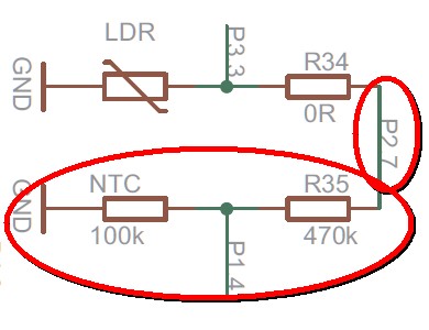
    The NTC implementation on the Experimenter Board also uses a GPIO pin P2.7 to source the NTC device (see below detail from circuit diagram, User Guide slau343b.pdf).
    NTC has 100k resistance and R35 has 470k resistance. This gives at room temperature a sum of 570k Ohm.

    In my NTC circuit I also use an NTC with 100k (at 25°C) but a smaller resistor (in place of R35) of 100k. So the sum is about 200k Ohm at room temperature (now 22°C). Using a power source with 3.6 V you would have a current of 0.018 mA which can easily be supplied from a GPIO pin. So the problem should not come from this side.

    On the board we have a regulated voltage (from TPS77301DGK) of Vcc = 3.67 V (measured).

    Measurement setup for my configuration:
    Power source from pin P2.5:                      Vcc       = 3.670 V            (Variation: +/- 0.010 V)
    Measuring NTC signal at pin P1.3:             Vsignal  = 1.760 V            (Variation: +/- 0.003 V)
    Vref is set to:                                                  Vref+     = Vcc = 3.670 V
                                                                             Vref
    -     = GND   (I guess this is equivalent to AVss)
    3.67 V / 1023 bit    results in                       3.587 mV/bit

    Further analysis:
    1. To check if the ADC is working well I have first connected the output pin P2.5 (3.670 V) to the analog input pin P1.5 to see the max. conversion result (full range signal at input pin).
       ADC10MEMO gives a value of 1022    (Variation: +/- 1;  during 50 measurements)
    This variation range of 2 units seems to me (at first sight) stable and OK.

    2. Connect the output pin P2.5 to power the NTC circuit with 3.67 V. Now I can measure an NTC signal of 1.760 V as input for pin P1.3. From that value I would expect a conversion result of                1.76/3.67 * 1023             =  491 units.
    But reading the ADC10MEMO register I get values varying from 454 to 547 (during 50 measurements).
    This is a variation range of 93 units (+56 / -37  with an equivalent of +200mV / - 133 mV). Compared to the range from case 1., it is about 50 times worse.

    3. When I drive the NTC circuit directly from Vcc on the board I get the same bad results as in case 2.

    4. When I look at the ADC10MEMO register running the “User experience” program for NTC temperature measurement (coming with the Experimenter Board), I see stable conversion results.

    5. I also connected the NTC circuit in the same way to a Launchpad with MSP430G2553. There I got the same unsatisfying results as described in point 2..

    Conclusions:
    A. Vcc seems to be stable enough (see 1.: very small variation in ADC result when P2.5 (Full span of 3.67 V) directly connected to P1.3 (Analog In)).
    B. Both, powering the NTC voltage divider circuit from GPIO pin or from Vcc shall be possible, because the current over the NTC circuit is very low (<< 0.1 mA).

    So what is still the problem when Vcc is stable enough and GPIO can power the low current of NTC circuit ???
    I have made a number of changes to ADC setting (e.g. sample + hold time variations, changing channels, changing GPIOs), all without positive effects.

    Solution:
    After hours of searching and reading, I found this posting from Jason Sachs:

         www.embeddedrelated.com/.../91.php&nbsp;

    Then I applied an R-C-Filter between the analog input pin and the signal from NTC.
    Incredible, that was it. The conversion result is now stable.

    Don’t know if TI has an application note describing the technique of filtering an analog signal before ADC. If you have please let me know. This could avoid a lot of trouble, perhaps for other users too.

    Helmut

  • Many thanks Leo, for your indications.
    Yes, the ADC settings are to have AVcc as VeREF+ and AVss as VeREF-.
    GND (AVss) is used for NTC circuit. It is the GND signal from the Experimenter Board MSP- EXP430FR5739, which I’m using.
    The solution now was to apply an R-C-Filter between the analog input pin and the signal from NTC.
    For more details please read my reply to Katie in the posting before.
    Helmut
  • Many thanks Katie for your indications.
    The tests are based on the Experimenter Board MSP- EXP430FR5739.
    The NTC implementation on the Experimenter Board also uses a GPIO pin P2.7 to source the NTC device (see below detail from circuit diagram, User Guide slau343b.pdf).
    NTC has 100k resistance and R35 has 470k resistance. This gives at room temperature a sum of 570k Ohm.

    In my NTC circuit I also use an NTC with 100k (at 25°C) but a smaller resistor (in place of R35) of 100k. So the sum is about 200k Ohm at room temperature (now 22°C). Using a power source with 3.6 V you would have a current of 0.018 mA which can easily be supplied from a GPIO pin. So the problem should not come from this side.
    On the board we have a regulated voltage (from TPS77301DGK) of Vcc = 3.67 V (measured).
    Measurement setup for my configuration:
    Power source from pin P2.5: Vcc = 3.670 V (Variation: +/- 0.010 V)
    Measuring NTC signal at pin P1.3: Vsignal = 1.760 V (Variation: +/- 0.003 V)
    Vref is set to: Vref+ = Vcc = 3.670 V
    Vref - = GND (I guess this is equivalent to AVss)
    3.67 V / 1023 bit results in 3.587 mV/bit
    Further analysis:
    1. To check if the ADC is working well I have first connected the output pin P2.5 (3.670 V) to the analog input pin P1.5 to see the max. conversion result (full range signal at input pin).
    ADC10MEMO gives a value of 1022 (Variation: +/- 1; during 50 measurements)
    This variation range of 2 units seems to me (at first sight) stable and OK.
    2. Connect the output pin P2.5 to power the NTC circuit with 3.67 V. Now I can measure an NTC signal of 1.760 V as input for pin P1.3. From that value I would expect a conversion result of 1.76/3.67 * 1023 = 491 units.
    But reading the ADC10MEMO register I get values varying from 454 to 547 (during 50 measurements).
    This is a variation range of 93 units (+56 / -37 with an equivalent of +200mV / - 133 mV). Compared to the range from case 1., it is about 50 times worse.
    3. When I drive the NTC circuit directly from Vcc on the board I get the same bad results as in case 2.
    4. When I look at the ADC10MEMO register running the “User experience” program for NTC temperature measurement (coming with the Experimenter Board), I see stable conversion results.
    5. I also connected the NTC circuit in the same way to a Launchpad with MSP430G2553. There I got the same unsatisfying results as described in point 2..
    Conclusions:
    A. Vcc seems to be stable enough (see 1.: very small variation in ADC result when P2.5 (Full span of 3.67 V) directly connected to P1.3 (Analog In)).
    B. Both, powering the NTC voltage divider circuit from GPIO pin or from Vcc shall be possible, because the current over the NTC circuit is very low (<< 0.1 mA).
    So what is still the problem when Vcc is stable enough and GPIO can power the low current of NTC circuit ???
    I have made a number of changes to ADC setting (e.g. sample + hold time variations, changing channels, changing GPIOs), all without positive effects.
    Solution:
    After hours of searching and reading, I found this posting from Jason Sachs:
    www.embeddedrelated.com/.../91.php
    Then I applied an R-C-Filter between the analog input pin and the signal from NTC.
    Incredible, that was it. The conversion result is now stable.
    Don’t know if TI has an application note describing the technique of filtering an analog signal before ADC. If you have please let me know. This could avoid a lot of trouble, perhaps for other users too.
  • Are you using a minimal sampling time of 9uS?

  • fritz01h said:
    The aim is to provide a stable power source for an NTC. Using simply the Vcc gives an unstable result.

    Vcc is usually stable enough to power NTC voltage divider if you also use Vcc as the reference for ADC. The ADC reading is the ratio and the exact voltage of Vcc does not matter much. That is why the arrangement on the FR5738 LP works.

    An accurate reference voltage is needed only if you want to measure voltage in absolute terms, which is not the case for a NTC voltage divider.

    The reference voltage source on your own board may react badly when the ADC takes samples. That is probably why you need to add RC in-between to soften the blow of ADC taking sample. 

  • Ref. to:

    An accurate reference voltage is needed only if you want to measure voltage in absolute terms, which is not the case for a NTC voltage divider.

    Yes, this is good to remember.

    Ref to:

    The reference voltage source on your own board may react badly when the ADC takes samples. That is probably why you need to add RC in-between to soften the blow of ADC taking sample. 

    But why do I get stable results when the AVcc is fed directly to the analog Input (disconnected NTC circuit) ? I would expect the same variation in the conversion result.  Because it is the same source and the same ADC configuration. This leads to the conclusion that the NTC circuit is the limiting part.

  • fritz01h said:
    But why do I get stable results when the AVcc is fed directly to the analog Input (disconnected NTC circuit) ? I would expect the same variation in the conversion result.  Because it is the same source and the same ADC configuration. This leads to the conclusion that the NTC circuit is the limiting part.

    Difference in series resistance = difference in ADC capacitor charging time!

  • This is the ADC configuration:
    ADC10CTL0 |= ADC10SHT_0 + ADC10ON; // ADC10ON, S&H=4 ADC clks
    ADC10CTL1 |= ADC10SHP; // ADCCLK = MODOSC; sampling timer
    ADC10CTL2 |= ADC10RES; // 10-bit conversion results
    ADC10MCTL0 |= ADC10INCH_3; // A3 ADC input select; Vref=AVCC
    ADC10IE |= ADC10IE0; // Enable ADC conv complete Interrupt
    So sampling period is 4 ADC clock cycles, which is the shortest sampling period avaiable.
    I have tested with all possible ADC10SHTx settings getting the same bad result.
    What is the idea behind your question?
  • Then you are using a wrong Sampling time, but your sampling time will not be the only error in your setup.

    For the Sampling time read the ‘User’s Guide’ section “16.2.5.3 Sample Timing Considerations” additional data you can find in the ‘Data Sheet’ “5.28 10-Bit ADC, Power Supply and Input Range Conditions” and further.

  • Sorry, but I have read both documents several times and it still seems not very clear to me.
    Could you give a concrete advice what to do.
  • The ADC connects to, and takes a snapshot (sample) of the to be measured voltage and stores this into a capacitor which, after disconnecting from the source/input, will be evaluated (converted) to a digital value.

    But as any capacitor (or maybe you understand better ‘battery’) the charge takes time, normally expressed in T=RxC.

    R is not a single resistor and C is not a single capacitor, in chapter 16.2.5.3 of the User’s Guide you see the equivalent of all of them.

    Some of the values are specific to the device which you can read in the Data Sheet other are depending on board/wiring capacitance and series resistor value (470K + 100K).

    From these parameters you need to calculate the minimum sample time needed for a good charge of the ADC capacitor to a representative voltage value. The time RxC gives you the time to a charge of ~63%, 5xRxC is near 100%, but for a more precise conversion result you need to take 8 (Tau) times (8xRxC).


    Maybe you now understand that when connecting your ADC input directly to your supply voltage the series resistance is very low and the capacitor charges fast, and just a short sampling time is needed. But in your NTC setup the series resistance is much larger and so the time needed to charge the capacitor much larger and a short sampling time is not sufficient to fully charge the capacitor.

    Buffering the NTC value with an extra capacitor connected to the ADC input pin will (partly) eliminate the NTC circuit resistance and a shorter sample time will work, but still needs to be calculated.

  • At the moment I’m too far away from being able to do the required calculations. But I understand that I have to increase the sample time to get the complete signal captured. So first l would like to continue configuring the ADC unit for longer sample periods.

    I have set the ADC10SHSx to max. value. The ADC conversion value is still changing too much.
    Then I set the ADC10DIVx to the highest value to see what happens. Yes, the value variation has now decreased. But the span is still not acceptable.
    Ok there is another chance to increase the sample time by setting ADCPDIVx to the highest value. Unfortunately also this gives not the desired result. The conversion value is not stable.

    I do not understand why the NTC circuit on the Experimenter Board works fine. It is also an NTC with 100 k resistance (see my earlier descriptions).

    Perhaps the best solution would be adding a unity-gain amplifier between NTC signal and analog input pin of the MCU.

    Regarding the required calculations, do you know some description that I could study to learn this?
    I also asked TI for an application note. No answer till now.

    Many thanks for your effort.

    Helmut

  • To increase precision, you may connect the port pin output to VeREF and use it for the ADC. This way, you eliminate the influence of the voltage drop on the port pin output.
    The main reason why the board uses a port pin to power the NTC is power consumption. When not actively measuring the temperature, you can pull the port pin low and the NTC won't draw any current.
    However, using the supply voltage of the NTC as reference makes the reading independent of the reference. But at the same time it means that you reduce resolution, since all the voltage across the top resistor is lost.

    Suggestion: make an Excel sheet where you have the NTC resistance at different temperatures, and the head resistance as variables and get the resolution (and expected ADC count). Then pick a head resistance so that you have your area of interest (the temperature range you want to cover) where your resolution is best.
    You may even extend the calculation by a parallel resistance to the NTC. If properly chose, you may get an almost linear reading in the area of interest.
    When using the internal 2.5V reference, this will increase resolution, as the voltage on the head resistor can be 1.1V with still full ADC resolution on the NTC voltage). But of course it reduces precision due to reference and supply not being the same (can be eliminated by measuring the supply too, e.g. by measuring VCC/2 with the ADC too)

    I don't like NTCs. I prefer a PTC (I just created a PTC circuit for a PT1000 in the temperature range of 0-100°C using a dual OpAMP as current source and offset eliminator. With a constant current, the voltage over the PTC is almost linear with temperature.
    But I too had to work with NTCs once. I used a parallel and head resistance, and a (calculated) lookup table for translating the ADC readings into temperature. I had to use the NTC because they were already built into the laser heads I was driving (it was a modulated laser supply with N-30A for 0-100% up to 30kHz modulation of an 8W green laser - precise temperature control was required for optimum efficiency and ray quality). Well, NTCs are cheap.
  • Katie,

    I want to use the external reference as an offset to an external amplifier with a single supply. But you said the internal reference cannot be used to drive another device? So what does this mean in Section 4.6?

    And this register description:

  • Hi Mike,

    What device are you using? The original post I answered above was about MSP430FR5739, but your datasheet screenshot does not appear to match this? Are you using MSP430FR5969 instead?

    On MSP430FR5739 if you look at the same section 4.6, you'll see that it only has VeREF+/- (designed to be inputs) available on pins, not VREF+/- as shown in your screenshot above (which appears to be from FR59xx part). If you are using the MSP430FR5969, the answer is different - in the MSP430FR5969 datasheet you can find the spec in section 5.12.5.5 Reference, that shows IO(VREF+) which is the VREF maximum load current on the VREF+ terminal that is allowed when you output the reference on the VREF+ pin. So yes, on MSP430FR5969 you can do this as long as you stay within this load current spec (-1000uA to +10uA load only).

    Regards,
    Katie
  • Ahh you are correct, I am using the FR5969 now, but had used the FR5739 previously on the project.  Thanks for the clarification!

  • If you enable REFOUT and use the reference externally, then be sure to have the recommended 100nF ceramic/10µF Tantalum combo between VRef+ and AVSS. On some devices, this is also necessary when you use higher sample rates, even if not using the reference for any external components.
    If current consumption is not a problem, I recommend using the TS431BCX or similar shunt regulator as external reference. It takes 1mA (you can tie it to an I/O pin for use on demand) but produces 2.495V +-0.5% which is way more precise than the internal 2.5V reference. And it i stable for even heavier loads - up to 100mA. But remember it's a shunt regulator. So it is a self-adjusting load that draws as much current from the source that the voltage breaks down to its reference voltage. You need to provide a proper head resistor between voltage source and regulator. I used this one a lot. It's cheap and small (SOT-5) and painless to use.

**Attention** This is a public forum