This thread has been locked.

If you have a related question, please click the "Ask a related question" button in the top right corner. The newly created question will be automatically linked to this question.

What does this section mean from the msp430x5xx users guide

Hi All,

Looking at the section below from msp430x5xx, what does "The block write must be initiated from RAM"? Does this mean that the code that is writing has to execute from RAM. Or does it mean that the source of the data needs to be from the RAM section?
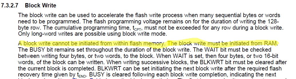
  • >Does this mean that the code that is writing has to execute from RAM?

    YES, I would also think that Source also have to be from RAM.

    If FLASH is locked from MCU's PC you would think it's looked from reads too.

  • AFAIK it means the code and the source data need to be in RAM, because reading flash is not possible during block write.

  • Hello Silver,

    Here is a very similar thread that I think answers your question:
    e2e.ti.com/.../262832

    From JMG: Code execution is only possible while doing a bank erase of a different bank. During write, no matter of which bank or segment erase, all flash access returns 0x3fff (not 0xfffe), which is indeed the JMP $ instruction but gives a bad ISR address. So block write can only be done from code running in ram, and with either the vector table redirected to ram and all ISRs in ram, or with interrupts disabled.

    Regards,
    Ryan

**Attention** This is a public forum