I am attempting to coordinate two chips to work together in order to write to a separate memory. The two chips I am working with are the N25Q00AA, a Serial NOR Flash Memory manufactured by Micron, and the MSP430FR5728, a MCU manufactured by TI. While working with these chips, I read through their data sheets as well as the following forum post:
While the discussion present there was somewhat helpful, I am still facing serious problems working with this.
The first problem faced is that, when attempting to use either of the following two lines of code, the project is stuck and unable to progress any further:
while ((UCB0IFG & UCTXIFG)== 0);
while ((UCB0IFG & UCRXIFG) == 0);
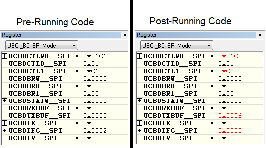
When I remove the “UCB0IFG” the code can run, however then I face a significant problem. The MSP430FR5728 fails to read anything from the N25Q00AA, and always outputs “0” when I attempt to print any values read.
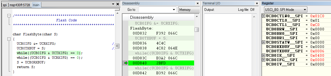
The following is the code that I use when trying to Read the Status Register.
char FlashByte(char S)
{
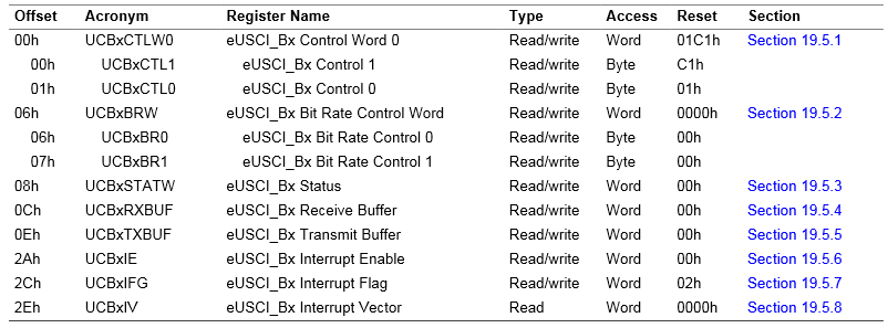
UCB0IFG &= UCRXIFG; // Clear RX Interupt
UCB0TXBUF = S; // Write Byte
while((UCB0IFG & UCTXIFG) == 0);
while((UCB0IFG & UCRXIFG) == 0);
S = UCB0RXBUF;
return S;
}
int main(void)
{
WDTCTL = WDTPW | WDTHOLD; // Stop watchdog timer
PMMCTL0 = PMMPW; // Open PMM Module
PM5CTL0 &= ~LOCKLPM5; // Clear locked IO Pins
PJDIR |= 0x02;
PJOUT |= 0x02;
// Configure SPI
UCB0CTL1 = UCSWRST; // Enabled
UCB0CTL0 |= UCCKPH + UCMSB + UCMST + UCSYNC; // 3 pin, 8-bit SPI mode?
UCB0CTL1 |= UCSSEL_2; // SMCLK
UCB0BR0 |= 0x00; // /2
UCB0BR1 = 0; // 1 MHz, 9600 Baud Rate
UCB0CTL1 &= ~UCSWRST;
for(;;)
{
PJOUT ^= BIT1;
FlashByte(0x06); // Write Enable Command
PJOUT ^= BIT1;
PJOUT ^= BIT1;
FlashByte(0x05); // Read Status Register Command, should output 0x02?
printf("check = %X\r\n",FlashByte(0xFF)); // Send dummy Byte, then print Status Register
PJOUT ^= BIT1;
}
}
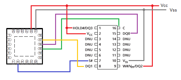
I will also attach a diagram detailing the connections I have created between the MSP430FR5728, and the N25Q00AA., which can be seen below:
I feel like if I could just be able to properly read the status register, I can then progress to the next step of trying to write to and read from the N25Q00AA without significant difficulty. If someone could help me to figure out what I am doing wrong, I would greatly appreciate the help