This thread has been locked.

If you have a related question, please click the "Ask a related question" button in the top right corner. The newly created question will be automatically linked to this question.

How to write new image into MSP430 flash?

Other Parts Discussed in Thread: MSP430BT5190

I'm new to the MSP430. I'm writing a boot loader. I accepting an image download then having to write the new executable image to the MSP430190 flash.

1. I have to write a primary boot loader. Does anyone have any example code?

2. Can I store the boot loader in BSL memory? If so does anyone have any example code on how to store code in BSL?

3. Has TI published any app notes regarding my concerns?

Thanks

  • Hi Ralph,

    Which MSP430 device are you using? Most MSPs already have a BSL in ROM or Flash in the device, so you could use that unless you needed something custom for some reason. We have a wide variety of BSL resources:

    Interfacing with TI MSP BSLs: www.ti.com/.../slau319 (1xx/2xx/4xx/5xx/6xx) - FRxx families have their own versions of this doc linked on their respective product pages
    Custom BSL for MSP430: www.ti.com/.../slaa450 (F5xx/6xx only - uses the BSL flash area available on these parts)
    MSP-BOOT: www.ti.com/.../slaa600 (all MSP430s - for doing a custom BSL in the main flash area - usually only used if you can't use the provided ROM BSL for some reason).

    There are more resources than this, but if we know what device you have and what are your requirements for your BSL (does it need to be a specific communication interface like UART/I2C/SPI, does it need to follow some existing host protocol, etc) then we can help guide you to which documents/resources are most relevant for your situation.

    Regards,
    Katie
  • Hi Katie,

    On the schematic the device is MSP430BT519. Here is what I have to do:

    Over the air download via blue tooth. Up to 1024 256 byte image packets received from the Bluetooth RF. The new image is stored in serial SPI flash. When all the packets are received and stored in serial SPI flash then a primary boot loader needs to be invoked to read each and all packets from the serial flash and over write (re-program) the MSP430 executable flash.

    I could put a small Primary Boot loader in SRAM, call it and it would read each packet from serial flash and program the CPU flash. Can I write the custom primary boot loader and locate it in BSL area? It would need to read packets from the external SPI serial flash and re-program the main CPU execution region. I need some C code examples of how to write a custom boot loader for BSL. Code examples in C  for programming main CPU flash memory.

    I need a person I can talk to or directly email. I know very little about this part but have done this kind of work with other Mfg's micro-controller parts.

    Thanks

  • Hi Ralph,

    Thank you for the additional information. The MSP430BT5190 comes with a UART based BSL in the BSL Flash. However you sound like you are needing a custom BSL because you need to read the data out of the SPI Flash when programming the device, rather than receiving it via UART.

    TI provides an app note and example code for creating your own custom BSL on F5xx devices - this is one of the things I already linked above, the Custom BSL app note www.ti.com/lit/pdf/slaa450 (the app note contains a link to the example code zip-file download as well). This describes how our BSLs are implemented and provides example projects - you could start with one of these example projects as a framework for your BSL code (it has a custom linker file set up to program into the BSL memory). The app note describes the structure used and should help you understand what the code does.

    Please note that the BSL area is only 2kB of flash. So implementing Bluetooth is probably not feasible in that area I would think. I'd recommend you go with a scheme of having the downloading code to the SPI flash over the air via Bluetooth as part of your main program, and then setting some signature (maybe have a CRC or code version number in the SPI Flash and the same in your code image, and compare to see if they match) that the device will be able to use to tell there's a new image in the SPI flash that needs to be loaded. Then jump to BSL in the BSL memory or reset the part. In the BSL_Protect function in the BSL430_low_level_init file, have it instead check for this version number/signature/CRC etc not matching to determine if BSL/code loading should start or not (instead of the method we have right now of checking for the SYSBSLIND to be set by the TEST/RST entry sequence). Then based on the rest of the BSL code we provide in SLAA450, you can implement a new Peripheral Interface layer to load from the SPI Flash instead of receiving data via UART.

    There are some other threads on this forum that talk about doing something similar (BSL firmware load from SPI flash) that could be helpful too if you search this forum. For example: https://e2e.ti.com/support/microcontrollers/msp430/f/166/p/266053/932932

    Regards,

    Katie

  • I wrote an over the air programming enabled system.  It is rather unique, the production image has both the bsl and the application, whereas the reprogramming image only has the application, you can see it here:

    There are some pretty cool ideas, for example, you can run the hex2cbor, and it will break your binary up into smaller sections, then you send a section at at time to the uC.  It is not yet 100% done, but most of it is working.

  • Thanks. This was helpful. I'm using the msp430BT5190. I was going to put the primary boot loader in segment D of flash memory. This leaves segments A,B and C for the main application image code. Do I have to sacrifice the entire segment D (64K) for my boot loader? Can I use just 16K of segment D and the remaining 48k for application image? If so how would I do that? Even a segment erase, erases all of the 64K segment with the dummy write to any address in the segment. Is there away to erase just 48K in a segment so I can write over it?

    Thanks
    Ralph
  • Hi Ralph,

    I'm not sure if your question was for Silver Diamond or for me, but in any case the smallest eraseable area of flash is a segment. Now I was unsure when you said "segment D" if you meant INFOD in INFO memory, or Bank D in main memory (which is made of many segments). Based on the size you mentioned (64k), you must mean Bank D.

    Bank D in main memory is 64k, but this is made up of smaller 512 byte segments (see the datasheet for MSP430BT5190 "Flash Memory" section on p. 18). So you should be able to erase only part of it by doing segment erases on Bank D (you'll just want to align your memory usage for BSL vs main app along the segment boundaries - best way to do this would probably be to modify the linker cmd file).

    Hope this helps,

    Katie

  • Ralph,

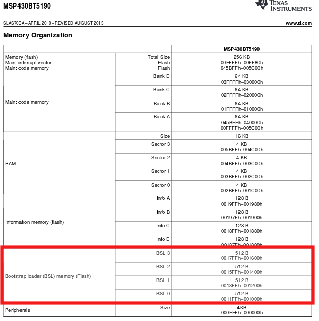
    You can do that, but my code is designed to go into the BSL memory region, below is the image from msp430bt5190 specifications, page 16 has the following:

    So the BSL region only has 2K of memory.  The repo that I am sharing has a little explanation that you need to allow the CCS to modify the contents of the BSL region.


    So to answer your questions, the BSL code that I published fits comfortably into 2K with level 1 size optimization, but, yes, if you do not optimize, it will not fit.  Also, it is based on thoroughly tested robust code.  You can erase memory in 512 byte sectors, except for the Information Memory (Info A through D) segments, you can erase these in 128 byte sectors, you never have to erase the full segments.  Hope this helps,

    cheers,

  • By the way if you look at:

    github.com/.../cBSL_main.c

    The line 8 and 98 forces the code into BSL. This places the cBSL_main() into the BSL segments.

    If you look at:

    github.com/.../BSL430_Low_Level_Init.asm

    line 18 calls the cBSL main form system startup. Once you are in the cBSL_main, you can erase, write-to flash, do a system reset or any other functions on the MCU.
  • Silver Diamond,

    Thanks for the reply. You sure seem like you know your stuff on the MSP430. I don't. It's a learning curve to me. I've been developing on this for 2 weeks now and the customer wants it fast. I've done OTA and serial downloads before but on STM8 and STM32 (ARM) micros. Different architectures and rules. Initially thought of using the BSL. Customizing the BSL but after I got into the document "Creating a Custom Flash-Based Bootstrap Loader (BSL)" it seemed quite involved and required assembly language. Z- area, etc. So my project manager and I agreed to just place a primary boot loader as high as possible in main CPU flash and jump to it after the OTA image is captured in SPI serial flash. We have decided to not use the BSL at this time and put the boot loader in high memory. Switch to the BSL at a later date.

    You say flash memory can be erased in 512 byte chunks. Everything I read says differently. Maybe its ambiguous to me and I'm misunderstanding.  My understanding is there are 4 64k segments of main memory in CPU flash (A-D). The erase to each segment is initiated by a dummy write to an address in that segment.  To erase in 512 byte chunks would I set FCTL1 the following way?

    FCTL1 = FWPW + MERAS;

    Its confusing to me as to how to configure the ERASE and MERAS bits to just do a 512 byte erase. If I could do that I could use most of segment D for application code and a small chunk for boot code.

    Thanks Ralph

    Below is my flash erase function.

    #define BANKA_DUMMY_WRITE_ADR    0x005C00
    #define BANKB_DUMMY_WRITE_ADR    0x010000
    #define BANKC_DUMMY_WRITE_ADR    0x020000

    void FlashMainMemoryErase(void)
    {
       unsigned char i;
       unsigned long DummySegAdr;
       char Ret = 0;
       unsigned long DummySegAdrs[] = {BANKA_DUMMY_WRITE_ADR,
                                       BANKB_DUMMY_WRITE_ADR,
                                       BANKC_DUMMY_WRITE_ADR};
                                       
       for(i = 0; i < 3; i++)
       {
           while (FCTL3 & BUSY);       // make sure CPU flash controller not busy
           FCTL3 = FWPW;                 // Clear Lock bit
           FCTL1 = FWPW + ERASE;         // Set Erase bit

           DummySegAdr = DummySegAdrs[i]; // Get address with bank

           __data20_write_char(DummySegAdr, 0); // Dummy write to start
                                                // erase Flash seg
           while (FCTL3 & BUSY);       // make sure controller not busy
           FCTL3 = FWKEY + LOCK;       // Lock controller
       }
    }

  • Hi Ralph,

    Ralph Sweitzer said:

    You say flash memory can be erased in 512 byte chunks. Everything I read says differently. Maybe its ambiguous to me and I'm misunderstanding.  My understanding is there are 4 64k segments of main memory in CPU flash (A-D). The erase to each segment is initiated by a dummy write to an address in that segment.  To erase in 512 byte chunks would I set FCTL1 the following way?

    FCTL1 = FWPW + MERAS;

    Its confusing to me as to how to configure the ERASE and MERAS bits to just do a 512 byte erase. If I could do that I could use most of segment D for application code and a small chunk for boot code.

    Please see the device family user's guide www.ti.com/lit/pdf/slau208 section 7.2. You can see a description of how each 64k Bank is further split into 512 byte segments - it is also explained in the datasheet for the device as I mentioned in my post above. It also explains that the smallest unit that can be erased is a segment (not a bank). Setting MERAS as you mention above is not correct - that will erase the whole 64k bank. Instead you should set only ERASE (as done in your code at the bottom of your post)

    When you test that function you posted is it not working for you? Looking at the FCTL1 register description in the device user's guide www.ti.com/lit/pdf/slau208 , in section 7.4.1 FCTL1 register, you can see that for Segment erase, you should have MERAS = 0 and ERASE = 1, vs for bank erase MERAS = 1 and ERASE = 0 (and if both are 1 then you'll have a mass erase of all memory segments). Comparing your code to that in section 7.3.1.4 of the same document which shows a segment erase example, it looks like it matches what you are doing to me. I think you would see the first segment of each bank being erased (since the addresses you've chosen are the first addresses of the bank).

    Regards,

    Katie

  • Ralph,

    Actually, if you take a look at the file:

    github.com/.../cBSL_hw_layer.h

    take a look at line 69, this is function I use, it is based on driverlib function. You can specify what you erase via msp430.h macros ERASE and MERAS. These values determine if you are mass erasing or sector erasing.
  • Silver Diamond,
    Thanks. Please correct me if I'm wrong. If my code is running out of high memory bank D I cannot erase any segments of in memory bank D.
    There is bank, sector within the bank and mass erase.
    I believe FCTL1 = FWPW+MERAS will erase a 512 byte segment in the bank if the dummy write is in that address of the segment.

    I looked at your BSL assembly code example . It uses Code Composer. I would have to adapt that to IAR which I am using.
    Ralph
  • Does anyone have BSL source code for the msp430BT5190? Include the .xcl file. Greatly appreciated if I can get that.

    Ralph

    Fuel7

  • Hi Ralph,

    The MSP430BT5190 has a UART BSL in the BSL memory. It should be the same source code as that of the MSP430F543xA BSL source code, that can be downloaded from: software-dl.ti.com/.../index_FDS.html

    Go into the folder 5xx_6xx_BSL_Source and you'll find the MSP430F543xA_TA_UART IAR project - this should be the same one that is in the BT5190.

    Regards,
    Katie

**Attention** This is a public forum