i am using MSP430G2553 for converting analog ECG into digital signal. in my analog hardware there are different stages like instrumentation amplifier,low pass filter,high pass filter, notch filter, dc offset adder circuit. for testing i am using sine wave. output at the end of dc offset circuit look like that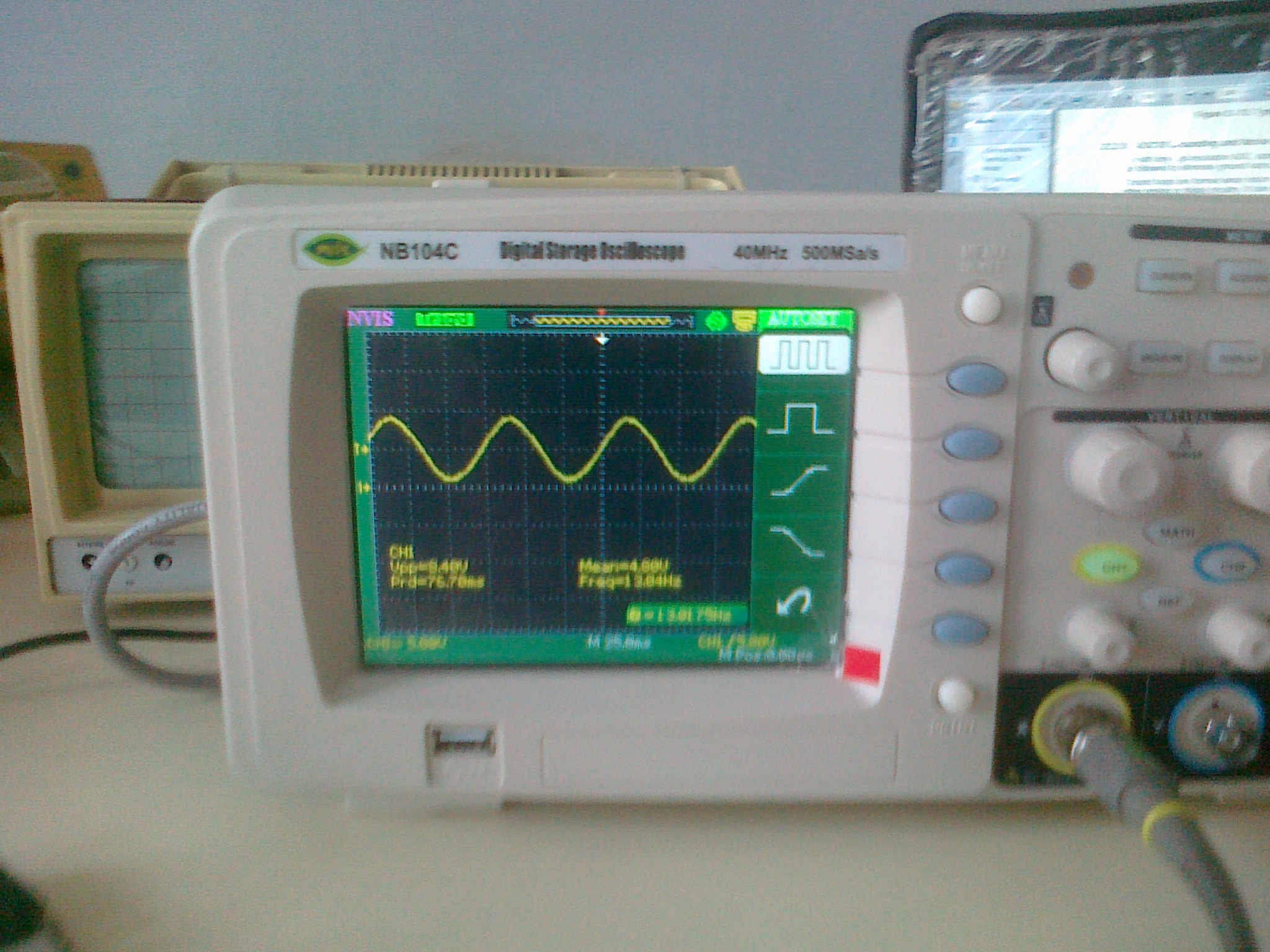
but when i connect this output to p1.1 which is my analog channel 1. in DSO my waveform look like below
when i put 10 uF capacitor before analog channel. shape of wave is better. but amplitude decreases. can you provide me solution?