Hello all,
I am attempting to work with a Flash Memory chip, and have so far only had negative results. I am attempting to work with the MSP430FR5728 by TI, and the S70FL01GS by Spansion.
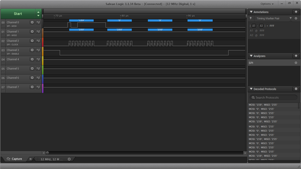
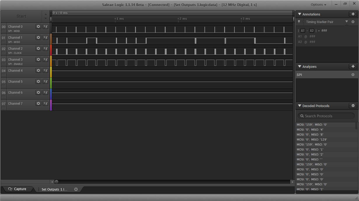
I am trying to perform the Read ID, however all of my attempts have resulted in either FFh or 00h.
I have been using a logic analyzer to see the results, and will post a screenshot below:
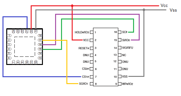
For the life of me I am not sure what I am doing wrong. I have read through the datasheets, and made sure the voltages and configurations matched that of what was needed. I even made sure that the circuit was wired correctly, as can be seen in the figure below.
I believe that everything is wired correctly for this simple task of Read ID. Below is also the code I wrote using IAR Embedded Workbench
/***********************************************************
Code Goal:  Write a Byte of data to address of S70FL01GS.
After which, read the same address to prove that the
data byte was properly recorded to the Flash Memory.

Read ID:  Datasheet says send command and then 3 dummy bytes

Write:  Datasheet states need to Enable Write, send 3 address
bytes, and requires the READ FLAG STATUS REGISTER command being
issued with at least one byte output.

Read: send 3 address bytes of where want to read

Program: IAR Embedded Workbench IDE
MCU: MSP430FR5728
SPI: B0 mode selected from device
UCB0SIMO: P1.6
UCB0S0MI: P1.7
UCB0CLK: P2.2
CSn 1: PJ.2
CSn 1: PJ.4

***********************************************************/

#include "string.h"
#include "msp430.h"
#include <stdio.h>

char b1 = 0x01;          // Flash Addr Part 1 for Write
char b2 = 0x02;          // Flash Addr Part 2 for Write
char b3 = 0x01;          // Flash Addr Part 3 for Write

char b4 = 0x01;          // Flash Addr Part 1 for Read
char b5 = 0x02;          // Flash Addr Part 2 for Read
char b6 = 0x01;          // Flash Addr Part 3 for Read

char Q;
char T;

unsigned char RXData =0;
unsigned char TXData;

char Readout[20];

/***************************************************
                     Flash Code
***************************************************/

char FlashByte(char S){       // General FlashByte Transmit
  __delay_cycles(60);
  UCB0TXBUF = S;
  while (!(UCB0IFG & UCTXIFG));
  S = UCB0RXBUF;
  while (!(UCB0IFG & UCRXIFG));
  return S;
}

char FlashComID(char S){       // Read ID command 9Fh
  PJOUT &= ~ BIT4;
  //while (!(UCB0IFG & UCTXIFG));
  UCB0TXBUF = S;                // Send Command
  while (!(UCB0IFG & UCTXIFG));
  while (!(UCB0IFG & UCRXIFG));
  UCB0TXBUF = 0x00;             // Dummy 1
  while (!(UCB0IFG & UCTXIFG));
  Readout[0] = UCB0RXBUF;       // Read 1
  while (!(UCB0IFG & UCRXIFG));
  UCB0TXBUF = 0x00;             // Dummy 2
  while (!(UCB0IFG & UCTXIFG));
  Readout[1] = UCB0RXBUF;       // Read 2
  while (!(UCB0IFG & UCRXIFG));
  UCB0TXBUF = 0x00;             // Dummy 3
  while (!(UCB0IFG & UCTXIFG));
  Readout[2] = UCB0RXBUF;       // Read 3
  while (!(UCB0IFG & UCRXIFG));
  PJOUT |= BIT4;
  return (UCB0RXBUF);
}

/***************************************************
                     Main Code
***************************************************/

int main(void){
  WDTCTL = WDTPW | WDTHOLD;                     // Stop watchdog timer

  PJDIR |= 0x1F;
  PJOUT |= 0x1F;


  // Clock Setup For SPI
  CSCTL0_H = 0xA5;
  CSCTL1 |= DCOFSEL0 + DCOFSEL1;                // Set DCO = 8MHz
  CSCTL2 = SELA_3 + SELS_3 + SELM_3;            // set ACLK = SMCLK = MCLK = DCO
  CSCTL3 = DIVA_1 + DIVS_1 + DIVM_1;            // ACLK = SMCLK = MCLK = 1MHz

  // Configure SPI
  P1SEL1 |= BIT6 + BIT7;                        // Set pins for primary purpose
  P2SEL1 |= BIT2;                               // Set pin for primary purpose
  UCB0CTLW0 |= UCSWRST;
  UCB0CTLW0 |= UCCKPH + UCMST + UCSYNC + UCMSB;
  UCB0CTLW0 |= UCSSEL_3;                    // SMCLK = 4MHz
  UCB0BR0 = 0x02;                           // /2
  UCB0BR1 = 0;                              //
  UCB0CTLW0 &= ~UCSWRST;


  for(;;){
    FlashComID(0x9F);
    __delay_cycles(500);
  }
}
Anyone have any ideas of what I might be doing wrong? Suggestions?
Thanks!


