This thread has been locked.

If you have a related question, please click the "Ask a related question" button in the top right corner. The newly created question will be automatically linked to this question.

Timer_D Issue


i tried to use Timer_D to implement two complimentary PWM with dead time control in high-res mode uisng F5132,but the pity is:

so i tried to use synchronized Timer0_D and Timer1_D with TDxCCR1 and TDxCCR2 combined,but the reslut is:

(1) the figure bellow is my code:

(2)when i used TimerD in normal mode(TDCLK = 16M),it peforms functionally as bellow

(3)when i used TimerD in high-res mode,it is not perform functionally(master is ok and slave not) just as bellow:

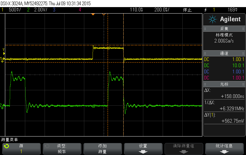
so i want ask TI employee, whether do this bug (synchronizing Timer0_D and Timer1_D with TDxCCR1 and TDxCCR2 combined  do not perform functionally)exist??? 

  • Kissn,
    I reproduced your results in the lab. I will send this to our systems team to verify the behavior. I should have an answer for you tomorrow.

    Thanks,
    Damian
  • Damain did my issue has been solved?
  • This issue is being resolved offline. Final results will be posted here when available.

    Damian
  • the code you sent to me do not work functionally when combined CCR1 and CCR2
  • I reproduced the problem in my lab and I was able to find a workaround. This seems to be a newly identified issue, so we need to do further analysis of the design of the device to understand the root of the problem, but hopefully the workaround helps you move forward with your work.  Here is what I found:


    1)     Adding a delay between the start of timer and the clear of timer fixes the synchronization


    TD0CTL0 |= MC_1 + TDCLR;        Doesn’t work (what I sent you yesterday)


    TD0CTL0 |= MC_1;                          This works!

    For(i=0; i<delay; i++);

    TD0CTL0 |= TDCLR;


    2)     The minimum value of ‘delay’ depends on the value of the input clock to the timer (in this case SMCLK). For SMCLK = 1MHz, delay = 1 fixes the problem. For SMCLK = 16MHz, delay has to be at least 12. This may vary across devices, so putting a higher value for the delay is safer.

    For(i=0; i<1; i++);             For 1MHz SMCLK

    For(i=0; i<12; i++)            For 16MHz SMCLK


    3)     Points 1 and 2 are enough to solve the problem as long as the multiply register of TD0 (master timer) is 8 (TD0HCTL0 |= TDHM_0). If the multiply is by 16 on TD0, then we also need to do a multiply by 16 in TD1. The hi resolution module of TD1 does not have to be enabled, only the TDHM_1 bit must be set.


        TD0HCTL0 =    TDHD_0                   // Divider to 1

                    + TDHM_1                  // Multiply by 16

                     + TDHREGEN                // Regulated mode

              + TDHEN;                  // Enable Hi-Res


    Then we must set it also in TD1HCTL0. Note that TDHEN for TD1 is NOT set:


    TD1HCTL0 = TDHM_1;                   // Multiply by 16

    Full code file is attached. 

    Damian

    /* --COPYRIGHT--,BSD_EX
     * Copyright (c) 2012, Texas Instruments Incorporated
     * All rights reserved.
     *
     * Redistribution and use in source and binary forms, with or without
     * modification, are permitted provided that the following conditions
     * are met:
     *
     * *  Redistributions of source code must retain the above copyright
     *    notice, this list of conditions and the following disclaimer.
     *
     * *  Redistributions in binary form must reproduce the above copyright
     *    notice, this list of conditions and the following disclaimer in the
     *    documentation and/or other materials provided with the distribution.
     *
     * *  Neither the name of Texas Instruments Incorporated nor the names of
     *    its contributors may be used to endorse or promote products derived
     *    from this software without specific prior written permission.
     *
     * THIS SOFTWARE IS PROVIDED BY THE COPYRIGHT HOLDERS AND CONTRIBUTORS "AS IS"
     * AND ANY EXPRESS OR IMPLIED WARRANTIES, INCLUDING, BUT NOT LIMITED TO,
     * THE IMPLIED WARRANTIES OF MERCHANTABILITY AND FITNESS FOR A PARTICULAR
     * PURPOSE ARE DISCLAIMED. IN NO EVENT SHALL THE COPYRIGHT OWNER OR
     * CONTRIBUTORS BE LIABLE FOR ANY DIRECT, INDIRECT, INCIDENTAL, SPECIAL,
     * EXEMPLARY, OR CONSEQUENTIAL DAMAGES (INCLUDING, BUT NOT LIMITED TO,
     * PROCUREMENT OF SUBSTITUTE GOODS OR SERVICES; LOSS OF USE, DATA, OR PROFITS;
     * OR BUSINESS INTERRUPTION) HOWEVER CAUSED AND ON ANY THEORY OF LIABILITY,
     * WHETHER IN CONTRACT, STRICT LIABILITY, OR TORT (INCLUDING NEGLIGENCE OR
     * OTHERWISE) ARISING IN ANY WAY OUT OF THE USE OF THIS SOFTWARE,
     * EVEN IF ADVISED OF THE POSSIBILITY OF SUCH DAMAGE.
     *
     *******************************************************************************
     *
     *                       MSP430 CODE EXAMPLE DISCLAIMER
     *
     * MSP430 code examples are self-contained low-level programs that typically
     * demonstrate a single peripheral function or device feature in a highly
     * concise manner. For this the code may rely on the device's power-on default
     * register values and settings such as the clock configuration and care must
     * be taken when combining code from several examples to avoid potential side
     * effects. Also see www.ti.com/grace for a GUI- and www.ti.com/msp430ware
     * for an API functional library-approach to peripheral configuration.
     *
     * --/COPYRIGHT--*/
    //******************************************************************************
    
    #include <msp430.h> 


    //#define BASIC_MODE
    #define MULT_16
    
    #define USE_DCO_16MHz
    //#define USE_DCO_8MHz
    //#define USE_DCO_1MHz
    
    void F5172_config_VCore(void);
    void SetVcoreUp(unsigned int level);
    void F5172_config_CLK(void);
    
    /*
     * main.c
     */
    void main(void) {
        WDTCTL = WDTPW | WDTHOLD;	// Stop watchdog timer
        F5172_config_VCore();			// Setup VCore to correct range for desired frequency
    
        F5172_config_CLK();
        P2SEL |= BIT0 + BIT3;
        P2DIR |= BIT0 + BIT3;
    
        TD0CTL0 = TDSSEL_2			// Use SMCLK
        		+ CNTL_0			// 16-bit timer
    			+ ID_0				// Divide by 1
    			+ MC_0;				// Halt timer
    
    #ifdef BASIC_MODE
        TD0CTL1 |= TDCLKM_0;		// TD clock is internal hi-res clock
    #else
        TD0CTL1 |= TDCLKM_1;		// TD clock is internal hi-res clock
        TD0HCTL1 |= TDHCLKCR;		// Needed for regulated mode with CLK > 15 M
    #endif
    
    #ifndef BASIC_MODE
        TD0HCTL0 = TDHFW   			// Fast wake up mode
        		+ TDHD_0 			// Divider to 1
    			+ TDHM_0			// Multiply by 16
    			+ TDHREGEN			// Regulated mode
    			+ TDHEAEN
    			+ TDHEN;			// Enable Hi-Res
    
    #ifdef MULT_16
        TD0HCTL0 |= TDHM_1;
        TD1HCTL0 = TDHM_1;			// Multiply by 16. Part of the workaround
    #endif
    
    
        TD1HCTL1 |= TDHCLKCR;		// Needed for regulated mode with CLK > 15 M
    
    #endif
    
        TD1CTL1 = TDCLKM_2;			// TD1 clock - AUX clock from master
        TEC1XCTL2 |= TECAXCLREN;	// Enable synchronized clear
    
        TD0CTL1 |= TD2CMB;
        TD0CCR0 = 200;
        TD0CCR1 = 40;
        TD0CCR2 = 80;
        TD0CCTL2 |= OUTMOD_7;		// Reset/Set
    
        TD1CTL1 |= TD2CMB;
        TD1CCR0 = 200;
        TD1CCR1 = 40;
        TD1CCR2 = 80;
        TD1CCTL2 |= OUTMOD_7;


    #ifndef BASIC_MODE
        int i = 0;
        TD0CTL0 |= MC_1;		// Reset/Set
        for (i=0;i<12;i++);		// Delay workaround
        TD0CTL0 |= TDCLR;		// Clear Timer to sync
    #else
        TD0CTL0 |= MC_1 + TDCLR;		// Reset/Set
    #endif
    
    
           while(1){


           }
    
    }
    
    void F5172_config_VCore(void)
    {
      //
      // Change core voltage one level at a time.
      //
      SetVcoreUp (0x01);
      SetVcoreUp (0x02);
      SetVcoreUp (0x03);
    }
    
    
    void SetVcoreUp(unsigned int level)
     {
       //
    	//	Configure VCORE register for desired core voltage level
    	//
       PMMCTL0_H = PMMPW_H;												 // Open PMM registers for write
       SVSMHCTL = SVSHE + SVSHRVL0 * level + SVMHE + SVSMHRRL0 * level;     // Set SVS/SVM high side new level
       SVSMLCTL = SVSLE + SVMLE + SVSMLRRL0 * level;						 // Set SVM low side to new level
        while ((PMMIFG & SVSMLDLYIFG) == 0);								 // Wait till SVM is settled
       PMMIFG &= ~(SVMLVLRIFG + SVMLIFG);								     // Clear already set flags
       PMMCTL0_L = PMMCOREV0 * level;								  		 // Set VCore to new level
       if ((PMMIFG & SVMLIFG))											 	 // Wait till new level reached
         while ((PMMIFG & SVMLVLRIFG) == 0);
       SVSMLCTL = SVSLE + SVSLRVL0 * level + SVMLE + SVSMLRRL0 * level;	 // Set SVS/SVM low side to new level
       PMMCTL0_H = 0x00;													 // Lock PMM registers for write access
     }


    void F5172_config_CLK(void)
    {
    
      //
      // Configure basic CLK registers. ACLK and DCO source = REF0. Select DCO range for required system frequency
      //
      UCSCTL3 = SELREF_2;                       // Set DCO FLL reference = REFO
      UCSCTL4 |= SELA_2;                        // Set ACLK = REFO
      __bis_SR_register(SCG0);                  // Disable the FLL control loop
      UCSCTL0 = 0x0000;                         // Set lowest possible DCOx, MODx
      UCSCTL1 = DCORSEL_7;                      // Select DCO range 25MHz operation
    
      //
      // Configure registers for 16MHz operation
      //
      #ifdef USE_DCO_16MHz
      UCSCTL2 = FLLD_1 + 487;                   // Set DCO Multiplier for 16MHz
                                                // (N + 1) * FLLRef = Fdco
                                                // (487 + 1) * 32768 = ~16MHz
                                                // Set FLL Div = fDCOCLK/2
      __bic_SR_register(SCG0);                  // Enable the FLL control loop
    
      //
      //  Worst-case settling time for the DCO when the DCO range bits have been  changed is n x 32 x 32 x f_MCLK / f_FLL_reference.
      //  See UCS chapter in 5xx UG for optimization.
      //
      __delay_cycles(500000);					// 32 x 32 x 16 MHz / 32,768 Hz ~ 500000 MCLK cycles for DCO to settle
      #endif // USE_DCO_16MHz
    
    
      #ifdef USE_DCO_8MHz
    
      UCSCTL2 = FLLD_1 + 243;                   // Set DCO Multiplier for 16MHz
                                                // (N + 1) * FLLRef = Fdco
                                                // (243 + 1) * 32768 = ~8MHz
                                                // Set FLL Div = fDCOCLK/2
      __bic_SR_register(SCG0);                  // Enable the FLL control loop
    
      // Worst-case settling time for the DCO when the DCO range bits have been
      // changed is n x 32 x 32 x f_MCLK / f_FLL_reference. See UCS chapter in 5xx
      // UG for optimization.
      // 32 x 32 x 8 MHz / 32,768 Hz ~ 250000 MCLK cycles for DCO to settle
      __delay_cycles(250000);
      #endif // USE_DCO_8MHz
    
      #ifdef USE_DCO_1MHz
        UCSCTL2 = FLLD_1 + 30;                   // Set DCO Multiplier for 16MHz
                                                // (N + 1) * FLLRef = Fdco
                                                // (30 + 1) * 32768 = ~1MHz
                                                // Set FLL Div = fDCOCLK/2
      __bic_SR_register(SCG0);                  // Enable the FLL control loop
    
      // Worst-case settling time for the DCO when the DCO range bits have been
      // changed is n x 32 x 32 x f_MCLK / f_FLL_reference. See UCS chapter in 5xx
      // UG for optimization.
      // 32 x 32 x 1 MHz / 32,768 Hz ~ 31250 MCLK cycles for DCO to settle
      __delay_cycles(31250);
      #endif // USE_DCO_1MHz
    
      #ifdef USE_VLO
      UCSCTL4 |= SELA_1 		// ACLK = VLO
      UCSCTL5 |= DIVA_1 		// ACLK/2
      #endif //USE_VLO
    
      //
      // Loop until XT1,XT2 & DCO stabilizes - In this case only DCO has to stabilize
      //
      do
      {
        UCSCTL7 &= ~(XT1LFOFFG + XT1HFOFFG + DCOFFG);
                                                // Clear XT2,XT1,DCO fault flags
        SFRIFG1 &= ~OFIFG;                      // Clear fault flags
      }while (SFRIFG1&OFIFG);                   // Test oscillator fault flag
    }
    
    
    // Timer0_D1 Interrupt Vector (TDIV) handler
    #if defined(__TI_COMPILER_VERSION__) || defined(__IAR_SYSTEMS_ICC__)
    #pragma vector=TIMER0_D1_VECTOR
    __interrupt void TIMER0_D1_ISR(void)
    #elif defined(__GNUC__)
    void __attribute__ ((interrupt(TIMER0_D1_VECTOR))) TIMER0_D1_ISR (void)
    #else
    #error Compiler not supported!
    #endif
    {
      switch(__even_in_range(TD0IV,30))
      {
        case  0: break;                          // No interrupt
        case  2: break;                          // CCR1 not used
        case  4: break;                          // CCR2 not used
        case  6: break;                          // reserved
        case  8: break;                          // reserved
        case 10: break;                          // reserved
        case 12: break;                          // reserved
        case 14: break;
        case 16: break;
        case 18:                                 // Clock fail low
          while(1);                              // Input ref clock freq too low; trap here
        case 20:                                 // Clock fail high
          while(1);                              // Input ref clock freq too high; trap here
        case 22:                                 // Hi-res freq locked
          // Hi-Res freq locked; now configure ports to output PWMs at TD0/TD1
          P1SEL |= BIT6 + BIT7;                  // P1.6/TD0.0, P1.7,TD0.1, options select
          P1DIR |= BIT6 + BIT7;                  // Output direction
          P2SEL |= BIT0 + BIT1 + BIT2 + BIT3;    // P2.0/TD0.2, P2.1/TD1.0, P2.2/TD1.1, P2.3/TD1.2, options select
          P2DIR |= BIT0 + BIT1 + BIT2 + BIT3;    // Output direction
    
          __bic_SR_register_on_exit(LPM0_bits + GIE);  // Exit LPM0 on return to main
    
          break;
        case 24: break;                          // Hi-res freq unlocked
        case 26: break;                          // reserved
        case 28: break;                          // reserved
        case 30: break;                          // reserved
        default: break;
      }
    }
    

**Attention** This is a public forum