This thread has been locked.

If you have a related question, please click the "Ask a related question" button in the top right corner. The newly created question will be automatically linked to this question.

MSP430g2553 pullup/down resistors not functioning as expected.

Other Parts Discussed in Thread: MSP430FR5969

So my project exposed an unexpected behavior in the g2553. 

the datasheet lists on page 328

"8.2.2 Output Registers PxOUT

Each bit in each PxOUT register is the value to be output on the corresponding I/O pin when the pin is
configured as I/O function, output direction, and the pullup/down resistor is disabled."


so in my mind if the "DIR" bit was set for a pin it would ignore the "REN" bit and just set the pin as an output.  however when it functions as the opposite,  if the REN bit is set, it becomes an input with the resistor set and ignores the "DIR" bit.


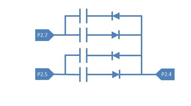
this is my setup on the project.  I have to check the state of 4 relay contacts using 3 input pins so they are charlieplexed with diodes.

so i enabled all 3 REN bits, and pulled P2.5 & P2.7 down and set P2.4 as an output high.  I was surprised to see the voltage at P2.4 was at 1.23V.  I disabled the REN bit for P2.4 only and it jumps up to 3.6V which is what I would have expected.

So with P2.4 having its DIR and OUT bits set when the REN bit is set it is now an input with the pullup resistor on (REN and OUT bits driving this)
this makes it 2 pulldown resistors and 1 pullup resistor feeding into the point, making a resistor divider and a voltage of 1.2V is about right.


I don't know if this is a known behavior but the datasheet leads me to believe the opposite should happen and the "DIR" bit will override the "REN" bit.

  • PxOUT will show at the Px pins under two conditions. (1) PxDIR is set, and (2) PxREN is disabled.

    You may set PxREN only when PxDIR is cleared.
  • There are two documents which describe mainly the MCU, the "User's Guide" and the "Datasheet". The User's Guide gives a general description of the MCU family group and the Datasheet gives specific information about the MCU used (and overrules in some cases the User’s Guide). Your reference to "8.2.2 Output Registers PxOUT" is not in the 'Datasheet' but in the 'User's Guide'.

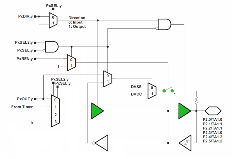
    In the Datasheet you can find the 'Port Schematics’. According to this schematic, your assumption is not correct. Also, a voltage divider cannot give here 1.2V but diode-Vf (diode voltage drop) less.

    I think there's something else going wrong.

  • Joseph Woodrell said:

    "8.2.2 Output Registers PxOUT

    Each bit in each PxOUT register is the value to be output on the corresponding I/O pin when the pin is
    configured as I/O function, output direction, and the pullup/down resistor is disabled."

    so in my mind if the "DIR" bit was set for a pin it would ignore the "REN" bit and just set the pin as an output.  however when it functions as the opposite,  if the REN bit is set, it becomes an input with the resistor set and ignores the "DIR" bit.

    That quote from the User's Guide doesn't say anything about what happens when the DIR and REN bits are both set, so I don't think you can conclude anything about which would override the other from this. That said, the next page has the following line:

    If the pin's pullup/pulldown resistor is enabled, the corresponding bit in the PxOUT register selects pullup
    or pulldown.
    Bit = 0: The pin is pulled down
    Bit = 1: The pin is pulled up

    That appears to match what you've observed, but there's a complication. I think this second quote only says that the pull resistor direction will be selected by PxOUT, but doesn't say that the output buffer won't also be enabled.

    The port schematics in the datasheet look like this for P2.4 and P2.5:

    So with PxDIR and PxREN both set, the output buffers and pull resistor (in green) should be both enabled. They both take the same value (from PxOUT), so the effect at the port pin should be effectively as if the resistor wasn't there.

    So now we're back where we started...

  • Ok, I've just done a quick test using the following code on the G2 launchpad:

    #include <msp430.h>
    
    void main()
    {
        WDTCTL = WDTPW | WDTHOLD;	// Stop watchdog timer
    
        P2OUT = BIT4 | BIT5;
        P2DIR = BIT4 | BIT5;
        P2REN = BIT4;
    
        __bis_SR_register(LPM4_bits);
    }

    I jumpered P2.4 and P2.5 to the two on-board LEDs. The LED powered by P2.4 is very weakly lit, while the one connected to P2.5 is bright. The same occurs if the code is modified to use P1.0 and P1.6, so it isn't port-specific.

    This confirms that having PxREN set disables the output buffer. That's consistent with what's written in the User's Guide, but doesn't match the port schematic.

    The same test on the MSP430FR5969 shows that on that chip PxDIR overrides PxREN (both LEDs are bright). That matches both the User's Guide and Datasheet for that chip.

  • So I now tested this as well and I can confirm this behaviour. If you do not connect a load to the pin, the output voltage does not change whether the PxREN is set or not. But if you connect a load to the pin, without having PxREN enabled, the output voltage drops only very little because of the driver's resistance. But when PxREN is then enabled with the load connected to the pin, the output voltage drops heavily.

**Attention** This is a public forum