Hi,
I am currently trying to establish communication between 2 MSP430G2553 launchpads with one configured as I2C master and the other as I2C slave. I referred to the example program given for MSP430G2553
1. msp430g2xx3_uscib0_i2c_04 (master) and
2. msp430g2xx3_uscib0_i2c_05 (slave)
I have made slight changes to example code for transmitting data.
I have configured SLAVE device to transmit data 0x00 and the MASTER device to recive it. The slave address is 0x7F.
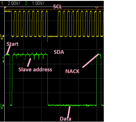
Referring to MSP430x2xx user guide it is said that the ACK bit is sent from the receiver after each byte on the 9th SCL clock pulse.The example code for I2C master has UCB0RXIE receive interrupt enabled, but the interrupt vector configured is for transmit (USCIAB0TX_VECTOR). I tried capturing the waveform for which both SCL and SDA are held low on the 9th clock pulse after the slave address is being transmitted. Further at the end of data transmission I get NACK. It seems that the master isnt receiving any data. .
Can anybody tell me if the vector configuration is correct or should the vector be USCIAB0RX_VECTOR.But when I tried configuring the vector to USCIAB0RX_VECTOR both SCL and SDA remains high all the time.
I2C MASTER CODE:
#include <msp430.h>
unsigned char RXData;
unsigned char RXCompare;
int main(void)
{
WDTCTL = WDTPW + WDTHOLD;
P1OUT &=~(BIT0+BIT1+BIT2+BIT3); // P1.0,p1.1,p1.2,p1.3 = 0
P1DIR |= 0x0f; // P1.0,p1.1,p1.2,p1.3 output
P1SEL |= BIT6 + BIT7; // Assign I2C pins to USCI_B0
P1SEL2|= BIT6 + BIT7; // Assign I2C pins to USCI_B0
UCB0CTL1 |= UCSWRST; // Enable SW reset
UCB0CTL0 = UCMST + UCMODE_3 + UCSYNC; // I2C Master, synchronous mode
UCB0CTL1 = UCSSEL_2 + UCSWRST; // Use SMCLK, keep SW reset
UCB0BR0 = 12; // fSCL = SMCLK/12 = ~100kHz
UCB0BR1 = 0;
UCB0I2CSA = 0x7F; // Slave Address is 0x7f
UCB0CTL1 &= ~UCSWRST; // Clear SW reset, resume operation
IE2 |= UCB0RXIE; // Enable RX interrupt
while (1)
{
while (UCB0CTL1 & UCTXSTP); // Ensure stop condition got sent
UCB0CTL1 |= UCTXSTT; // I2C start condition
while (UCB0CTL1 & UCTXSTT); // Start condition sent?
UCB0CTL1 |= UCTXSTP; // I2C stop condition
__bis_SR_register(CPUOFF + GIE); // Enter LPM0 w/ interrupts
}
}
// USCI_B0 Data ISR
#pragma vector = USCIAB0TX_VECTOR
__interrupt void USCIAB0TX_ISR(void)
{
P1OUT = UCB0RXBUF; // Get RX data
__bic_SR_register_on_exit(CPUOFF); // Exit LPM0
}
I2C SLAVE CODE:
#include <msp430.h>
unsigned char TXData;
int main(void)
{
WDTCTL = WDTPW + WDTHOLD; // Stop WDT
P1DIR |= BIT0; // P1.0 output
P1SEL |= BIT6 + BIT7; // Assign I2C pins to USCI_B0
P1SEL2|= BIT6 + BIT7; // Assign I2C pins to USCI_B0
UCB0CTL1 |= UCSWRST; // Enable SW reset
UCB0CTL0 = UCMODE_3 + UCSYNC; // I2C Slave, synchronous mode
UCB0I2COA = 0x7F; // Own Address is 0x7f
UCB0CTL1 &= ~UCSWRST; // Clear SW reset, resume operation
UCB0I2CIE |= UCSTTIE; // Enable STT interrupt
IE2 |= UCB0TXIE+ UCB0RXIE; // Enable TX & RX interrupt
TXData = 0x00; // Used to hold TX data, transmit data 0x00;
while (1)
{
__bis_SR_register(CPUOFF + GIE); // Enter LPM0 w/ interrupts
}
}
// USCI_B0 Data ISR
#pragma vector = USCIAB0TX_VECTOR
__interrupt void USCIAB0TX_ISR(void)
{
UCB0TXBUF = TXData; // TX data
__bic_SR_register_on_exit(CPUOFF); // Exit LPM0
}
I have attached the waveform output from my program. slave address is 0x7f and transmitted data is 0x00. 
Kindly tell me if there is any mistake in the coding
Thanks in advance...

