This thread has been locked.

If you have a related question, please click the "Ask a related question" button in the top right corner. The newly created question will be automatically linked to this question.

DMA9 erratta with SPI

Other Parts Discussed in Thread: MSP430F6779A

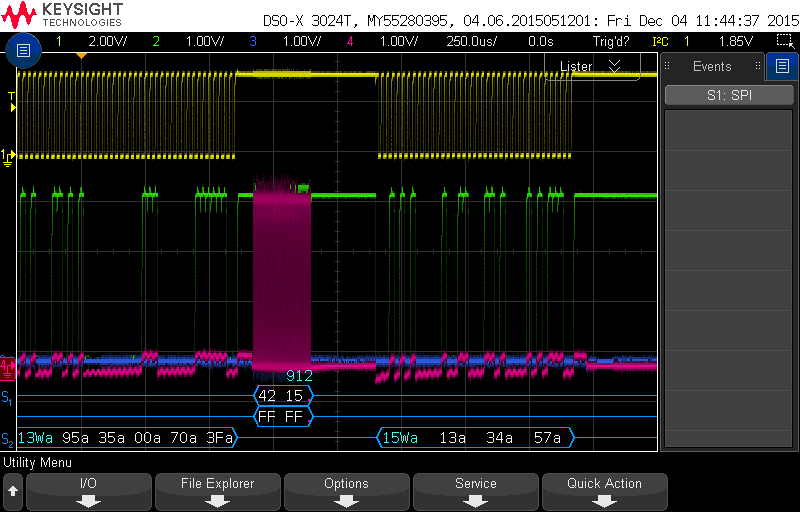
I am using the DMA and SPI to transfer data between two MSP430F6779A's.

I am sending 114 bytes at a time and most of the time it works but sometimes it sends fewer bytes than it should.

After looking at the erratasheet I suspect that I am running into DMA9. One of the suggested workarounds to use a second DMA channel of lower priority. I don't quite understand how this would work for two reasons:

1) I am seeing partial packets being sent which means that the second DMA channel needs to know how many bytes to send based on how far the first one got. I don't think this is possible

2) for the SPI master I need to both transmit and recive which uses two DMA channels so with the workaround I would need 4 DMA channels but, the MSP430F6779A only has 3.

Can someone tell me if this is what DMA9 looks like and how to properly implement the workaround as described in the erratasheet?

The errata claims that this is fixed in RevC of this chip. All my chips are RevB. Is there a way to purchase RevC chips? This would be ideal as I could avoid this annoying bug.

  • Hi Jesse,

    1) The job of the second DMA is not to send the bytes that are failed by the first DMA. Rather the idea is to unlock a hanging DMA channel with the 2nd channel. The source address and the destination address could be some dummy addresses and the size only needs to be set to 1. It’s not that you transfer the eUSCI data twice or in parallel. It’s more that the internal signal “hold_eset_del” will be cleared by the 2nd DMA channel. That is why the triggers are the exact same and the priority of the second DMA is lower than the first.

    2) If you know that you will not be sending and receiving at the same time you can alternate the dummy DMA's trigger between the RX and TX IFGs while keeping it at the lowest priority to service both RX and TX DMAs. Otherwise you will be forced to only use the DMA for SPI transmit or receive.

    This errata is indeed fixed in Rev C, you would have to specify which revision you want when ordering the devices to see if they are available.

    Regards,
    Ryan
  • Ryan,
    Thanks for the information I didn't quite get what the workaround was telling me. For a SPI master that only needs to receive data sending is mandatory so 2 DMA's are required. Right now on the master side I have the following:
    DMA0 -> USCIA0RX
    DMA1 -> USCIA0TX
    DMA2 -> USCIA0RX
    DMA0 and DMA1 are used to write data to the SPI and DMA2 writes to a dummy location. I am still seeing the same errors that I was without DMA2 enabled. I have also tried triggering DMA2 off of USCIA0TX with similar results. It seems to me that the workaround doesn't work or I am doing something wrong.

    I looked at the ordering page for the MSP430F6779A and saw nowhere to specify revision. How would one do this?

    Thanks,
    Jesse
  • Hi Jesse,

    Assuming that you are only experiencing difficulty receiving bytes but not sending then you are correct to focus DMA2 to trigger off of USCIA0RX. Don't you mean DMA0 is used to receive data from the SPI MISO line? The DMA9 workaround has been proven to work properly several times before, perhaps you can provide your DMA initialization code so that I can assist you further.

    You would need to contact a TI sales representative to ensure the revision being received.

    Regards,
    Ryan
  • The most visible difficulty that I am seeing is that occasionally the SPI peripheral does not clock out enough bytes for the entire transaction. Occasionally I see a bad CRC which could be from not sending enough bytes on the Slave side. I have tried triggering DMA2 from the TX but I didn't notice any difference.

    Yes I guess I misspoke a bit, DMA0 is used to read bytes from the SPI RXBUF and DMA1 is used to write bytes into the SPI TXBUF.

    Below is the initialization code for the DMA on the master side. SPI_buf is the pointer to the receive buffer and arcBus_stat.spi_stat.len is the packet length. In the tests I have done packet length has always been 112.

                  //============[setup DMA for transfer]============
                  //setup source trigger
                  DMACTL0 &=~(DMA0TSEL_15|DMA1TSEL_15);
                  DMACTL0 |= (DMA0TSEL__USCIA0RX|DMA1TSEL__USCIA0TX);
                  DMACTL1 = DMA2TSEL__USCIA0RX;
                  //setup dummy channel: read and write from dummy byte
                  *((unsigned int*)&DMA2SA) = (unsigned short)(&SPI_dummy);
                  *((unsigned int*)&DMA2DA) = (unsigned short)(&SPI_dummy);
                  // size isn't supposed to really matter
                  DMA2SZ = 10;
                  // Configure the DMA transfer, single byte transfer with no increment
                  DMA2CTL = DMADT_0|DMASBDB|DMAEN|DMASRCINCR_0|DMADSTINCR_0;
    
                  // Source DMA address: receive register.
                  *((unsigned int*)&DMA0SA) = (unsigned short)(&UCA0RXBUF);
                  // Destination DMA address: rx buffer.
                  *((unsigned int*)&DMA0DA) = (unsigned short)SPI_buf;
                  // The size of the block to be transferred
                  DMA0SZ = arcBus_stat.spi_stat.len+BUS_SPI_CRC_LEN;
                  // Configure the DMA transfer, single byte transfer with destination increment
                  DMA0CTL = DMAIE|DMADT_0|DMASBDB|DMAEN|DMASRCINCR_0|DMADSTINCR_3;
    
                  // Source DMA address: SPI transmit buffer, constant data will be sent
                  *((unsigned int*)&DMA1SA) = (unsigned int)(&UCA0TXBUF);
                  // Destination DMA address: the transmit buffer.
                  *((unsigned int*)&DMA1DA) = (unsigned int)(&UCA0TXBUF);
                  // The size of the block to be transferred
                  DMA1SZ = arcBus_stat.spi_stat.len+BUS_SPI_CRC_LEN-1;
                  // Configure the DMA transfer, single byte transfer with no increment
                  DMA1CTL=DMADT_0|DMASBDB|DMAEN|DMASRCINCR_0|DMADSTINCR_0;
                  //write the Tx buffer to start transfer
                  UCA0TXBUF=BUS_SPI_DUMMY_DATA;

    Below is a screen capture of what should be seen from the SPI. The packet that is beeing sent is 114 bytes long and results in 912 SPI clocks.

    The picture below shows what happens when it goes wrong. In this case the SPI only runs for 96 clocks or 12 bytes. This results in the DMA interrupt not happening screwing up the code later.

  • I was able to pull up a previous customer issue, here was the implemented workaround for receive:

    	// DMA initialization
    	DMA1CTL &= 0;// disable DMA channel 1
    	DMACTL0 = DMA1TSEL_22;// select UCB0RXIFG dma trigger for dma ch.1
    	DMA1CTL |= DMADSTINCR_3;// increment dest. addr after dma
    	DMA1CTL |= (DMADSTBYTE + DMASRCBYTE);// byte by byte transfer
    	DMACTL4 |= DMARMWDIS;
    	DMA1SZ = size;
    	dma1_completed = 0;
    	__data16_write_addr((unsigned short) &DMA1SA, (unsigned int) &UCB0RXBUF);// set DMA src address register
    	__data16_write_addr((unsigned short) &DMA1DA, (unsigned int) dst);// set DMA dst address register
    	DMA2CTL &= 0; // disable DMA channel 2
    	DMACTL0 |= DMA2TSEL_22;// select UCB0RXIFG dma trigger for dma ch.2
    	DMA2CTL |= (DMADSTBYTE + DMASRCBYTE);// byte by byte transfer
    	DMA2SZ = 1; /* One byte only */
    	/* Src/Dst dummy byte sets on unused register space on eUSCIA0 & eUSCIA1 (base address + 0x4) */
    	__data16_write_addr((unsigned short) &DMA2SA, (unsigned int) (0x05C0 + 0x0004));
    	__data16_write_addr((unsigned short) &DMA2DA, (unsigned int) (0x05E0 + 0x0004));
    	DMA2CTL |= DMADT_4 | DMAEN;// repeated single transfer, interrupts not needed for ch.2
    	DMA1CTL |= DMADT_4 | DMAIE | DMAEN; // enable dma interrupt 1ch

    And for transmit:

    	// DMA initialization
    	DMA1CTL &= 0;// disable DMA channel 1
    	DMACTL0 = DMA1TSEL_23;// select UCB0TXIFG dma trigger for dma ch.1
    	DMA1CTL |= DMASRCINCR_3;// increment src. addr after dma
    	DMA1CTL |= (DMADSTBYTE + DMASRCBYTE);// byte to byte transfer
    	DMACTL4 |= DMARMWDIS;
    	DMA1SZ = size;
    	dma1_completed = 0;
    	__data16_write_addr((unsigned short) &DMA1DA, (unsigned int) &UCB0TXBUF);// set DMA dst address register
    	__data16_write_addr((unsigned short) &DMA1SA, (unsigned int) src);// set DMA src address register
    	DMA2CTL &= 0; // disable DMA channel 2
    	DMACTL0 |= DMA2TSEL_23;// select UCB0TXIFG dma trigger for dma ch.2
    	DMA2CTL |= (DMADSTBYTE + DMASRCBYTE);// byte by byte transfer
    	DMA2SZ = 1; /* One byte only */
    	/* Src/Dst dummy byte sets on unused register space on eUSCIA0 & eUSCIA1 (base address + 0x4) */
    	__data16_write_addr((unsigned short) &DMA2SA, (unsigned int) (0x05C0 + 0x0004));
    	__data16_write_addr((unsigned short) &DMA2DA, (unsigned int) (0x05E0 + 0x0004));
    	DMA2CTL |= DMADT_4 | DMAEN;// repeated single transfer, interrupts not needed for ch.2
    	DMA1CTL |= DMADT_4 | DMAIE | DMAEN; // enable dma and dma interrupt

    Let me know if this helps for your application.

    Regards, Ryan

  • This code looks fairly similar to the code I have. Is there anything in particular that I should be paying attention to?

    I did see that their code sets DMARMWDIS which I added to my code and I see no changes in behavior.

    The biggest change is that they set the DMA to be in repeated single transfer mode whereas my code uses single transfer mode. I only want to receive a single block of data so I left DMA0 in single transfer mode and changed DMA2 to repeated single transfer mode. This didn't seem to change things either.

    One thing I noticed is that on line 12 of both segments DMACTL0 is set to configure DMA2. From reading the 5xx/6xx userguide this should be DMACTL1 because DMACTL0 is used to configure DMA0 and DMA1. Is there a reason for this? What channel is DMA2 configured for then? The default state of DMCATL1 is zero which corresponds to DMAREQ. I switched DMA2 to trigger off of DMAREQ which drastically reduced the number of screw ups but did not completely eliminate them.

  • I apologize, this is an error in the example. It should be DMACTL1 |= DMA2TSEL_23; to correctly set DMA2. DMAREQ is software-controlled and will not be triggered unless manually set inside of the DMAxCTL register. I do not know how it reduces the number of faults since it does not implement the DMA9 workaround correctly. Make sure that your dummy source and destination addresses are not the same just in case this is causing an error with the DMA, and also change your dummy DMA size to 1 byte and see if that results in any improvements.

    Regards,
    Ryan
  • I changed the DMA source and destination addresses to point to unused peripheral space and switched DMA2 back to USCIA0RX and it is working as it should now. Below is the final code:

                  //============[setup DMA for transfer]============
                  //setup source trigger
                  DMACTL0 &=~(DMA0TSEL_31|DMA1TSEL_31);
                  DMACTL0 |= (DMA0TSEL__USCIA0RX|DMA1TSEL__USCIA0TX);
                  DMACTL1 = DMA2TSEL__USCIA0RX;
                  //setup dummy channel: read and write from unused space on the USCI registers
                  *((unsigned int*)&DMA2SA) = EUSCI_A0_BASE + 0x04;
                  *((unsigned int*)&DMA2DA) = EUSCI_A1_BASE + 0x04;
                  // only one byte
                  DMA2SZ = 1;
                  // Configure the DMA transfer, repeated byte transfer with no increment
                  DMA2CTL = DMADT_4|DMASBDB|DMAEN|DMASRCINCR_0|DMADSTINCR_0;
    
                  // Source DMA address: receive register.
                  *((unsigned int*)&DMA0SA) = (unsigned short)(&UCA0RXBUF);
                  // Destination DMA address: rx buffer.
                  *((unsigned int*)&DMA0DA) = (unsigned short)SPI_buf;
                  // The size of the block to be transferred
                  DMA0SZ = arcBus_stat.spi_stat.len+BUS_SPI_CRC_LEN;
                  // Configure the DMA transfer, single byte transfer with destination increment
                  DMA0CTL = DMAIE|DMADT_0|DMASBDB|DMAEN|DMASRCINCR_0|DMADSTINCR_3;
    
                  // Source DMA address: SPI transmit buffer, constant data will be sent
                  *((unsigned int*)&DMA1SA) = (unsigned int)(&UCA0TXBUF);
                  // Destination DMA address: the transmit buffer.
                  *((unsigned int*)&DMA1DA) = (unsigned int)(&UCA0TXBUF);
                  // The size of the block to be transferred
                  DMA1SZ = arcBus_stat.spi_stat.len+BUS_SPI_CRC_LEN-1;
                  // Configure the DMA transfer, single byte transfer with no increment
                  DMA1CTL=DMADT_0|DMASBDB|DMAEN|DMASRCINCR_0|DMADSTINCR_0;
                  //write the Tx buffer to start transfer
                  UCA0TXBUF=BUS_SPI_DUMMY_DATA;

    Thanks,

    Jesse

**Attention** This is a public forum