This thread has been locked.
If you have a related question, please click the "Ask a related question" button in the top right corner. The newly created question will be automatically linked to this question.
Hi,
I am currently trying to set up a master-slave communication via i2c between an msp432p401r (master) and an msp430f5529 (slave). I am using modified example problems for each (attached). The code is far from complete as I haven't tested anything beyond the initial i2c start command. The slave interrupts the master via a GPIO pin to trigger the gpio_isr which calls the driverlib command:
MAP_I2C_masterReceiveStart(EUSCI_B0_MODULE);
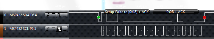
At this point, I get a NACK response from the slave (see photo below). However, for this test, the slave register UCB1I2COA is set to 0x49, and UCB0I2CSA on the master is set to 0x49, so this should acknowledge? As a result, the euscib0_isr function never runs.
Maybe it's a simple problem that I'm just not seeing. Have I configured the interrupt incorrectly? Could anybody please help?
Thanks,
Jordan
/* * ------------------------------------------- * MSP432 DriverLib - v2_20_00_08 * ------------------------------------------- * * --COPYRIGHT--,BSD,BSD * Copyright (c) 2014, Texas Instruments Incorporated * All rights reserved. * * Redistribution and use in source and binary forms, with or without * modification, are permitted provided that the following conditions * are met: * * * Redistributions of source code must retain the above copyright * notice, this list of conditions and the following disclaimer. * * * Redistributions in binary form must reproduce the above copyright * notice, this list of conditions and the following disclaimer in the * documentation and/or other materials provided with the distribution. * * * Neither the name of Texas Instruments Incorporated nor the names of * its contributors may be used to endorse or promote products derived * from this software without specific prior written permission. * * THIS SOFTWARE IS PROVIDED BY THE COPYRIGHT HOLDERS AND CONTRIBUTORS "AS IS" * AND ANY EXPRESS OR IMPLIED WARRANTIES, INCLUDING, BUT NOT LIMITED TO, * THE IMPLIED WARRANTIES OF MERCHANTABILITY AND FITNESS FOR A PARTICULAR * PURPOSE ARE DISCLAIMED. IN NO EVENT SHALL THE COPYRIGHT OWNER OR * CONTRIBUTORS BE LIABLE FOR ANY DIRECT, INDIRECT, INCIDENTAL, SPECIAL, * EXEMPLARY, OR CONSEQUENTIAL DAMAGES (INCLUDING, BUT NOT LIMITED TO, * PROCUREMENT OF SUBSTITUTE GOODS OR SERVICES; LOSS OF USE, DATA, OR PROFITS; * OR BUSINESS INTERRUPTION) HOWEVER CAUSED AND ON ANY THEORY OF LIABILITY, * WHETHER IN CONTRACT, STRICT LIABILITY, OR TORT (INCLUDING NEGLIGENCE OR * OTHERWISE) ARISING IN ANY WAY OUT OF THE USE OF THIS SOFTWARE, * EVEN IF ADVISED OF THE POSSIBILITY OF SUCH DAMAGE. * --/COPYRIGHT--*/ /******************************************************************************* * MSP432 I2C - EUSCI_B0_MODULE I2C Slave Initiated Read from Master * * Description: This example demonstrates the use case where the slave needs * to initiate a transfer from the master. This is often done in sensor * applications and other applications where the slave has to progressively * send data to the master when there is new data (perhaps from a sensor) to * be sent. A GPIO port is used to wake-up the master and initiate the * master to read data from the slave. In this case, the first byte of the * master read will be the number of bytes (including the length byte) that * the master should read. The GPIO pin is set as an input with a pull-up * enabled. This is the MASTER code. * * ACLK = n/a, MCLK = HSMCLK = SMCLK = BRCLK = default DCO = ~3.0MHz * * /|\ /|\ * MSP432P401 10k 10k MSP432P401 * slave | | master * ----------------- | | ----------------- * | P1.6/UCB0SDA|<-|----+->|P1.6/UCB0SDA | * | | | | | * | | | | | * | P1.7/UCB0SCL|<-+------>|P1.7/UCB0SCL | * | | | | * | P1.0/GPIO|<-------->|P1.0/GPIO | * | | | | * * Author: Timothy Logan ******************************************************************************/ /* DriverLib Includes */ #include "driverlib.h" /* Standard Includes */ #include <stdint.h> #include <stdbool.h> /* Slave Address */ #define SLAVE_ADDRESS_1 0x48 #define SLAVE_ADDRESS_2 0x49 #define SLAVE_ADDRESS_3 0x50 /* Statics */ static volatile uint8_t RXData1[4]; static volatile uint8_t RXData2[4]; static volatile uint8_t RXData3[4]; static volatile uint32_t xferIndex; static volatile uint32_t numOfRecBytes; static volatile uint8_t ReadFromSlaveAddress; /* I2C Master Configuration Parameter */ const eUSCI_I2C_MasterConfig i2cConfig = { EUSCI_B_I2C_CLOCKSOURCE_SMCLK, // SMCLK Clock Source 3000000, // SMCLK = 3MHz EUSCI_B_I2C_SET_DATA_RATE_100KBPS, // Desired I2C Clock of 400khz 0, // No byte counter threshold EUSCI_B_I2C_NO_AUTO_STOP // No Autostop }; int main(void) { /* Disabling the Watchdog */ MAP_WDT_A_holdTimer(); xferIndex = 0; /* Select Port 1 for I2C - Set Pin 6, 7 to input Primary Module Function, * (UCB0SIMO/UCB0SDA, UCB0SOMI/UCB0SCL). and setting P1.0 for input mode * with pull-up enabled */ MAP_GPIO_setAsPeripheralModuleFunctionInputPin(GPIO_PORT_P1, GPIO_PIN6 + GPIO_PIN7, GPIO_PRIMARY_MODULE_FUNCTION); //MAP_GPIO_setAsInputPinWithPullUpResistor(GPIO_PORT_P1, GPIO_PIN0); /* Setting GPIO pins 4.1,5.1 and 6.1 as inputs with pull-up resistors, allowing a high-to-low transition to trigger an ISR which will read code from the slave with specific address*/ P4REN |= BIT1; // Enable P4.1 internal resistance P4OUT |= BIT1; // Set P4.1 as pull-Up resistance P4IES |= BIT1; // P4.1 Hi/Lo edge P4IFG &= ~BIT1; // P4.1 IFG cleared P4IE |= BIT1; // P4.1 interrupt enabled P5REN |= BIT1; // Enable P5.1 internal resistance P5OUT |= BIT1; // Set P5.1 as pull-Up resistance P5IES |= BIT1; // P5.1 Hi/Lo edge P5IFG &= ~BIT1; // P5.1 IFG cleared P5IE |= BIT1; // P5.1 interrupt enabled P6REN |= BIT1; // Enable P6.1 internal resistance P6OUT |= BIT1; // Set P6.1 as pull-Up resistance P6IES |= BIT1; // P6.1 Hi/Lo edge P6IFG &= ~BIT1; // P6.1 IFG cleared P6IE |= BIT1; // P6.1 interrupt enabled /* Initializing I2C Master to SMCLK at 400kbs with no autostop */ MAP_I2C_initMaster(EUSCI_B0_MODULE, &i2cConfig); MAP_I2C_setSlaveAddress(EUSCI_B0_MODULE,SLAVE_ADDRESS_1); /* Set in receive mode */ MAP_I2C_setMode(EUSCI_B0_MODULE, EUSCI_B_I2C_RECEIVE_MODE); /* Clearing interrupts for I2C and enabling the module */ MAP_I2C_enableModule(EUSCI_B0_MODULE); MAP_I2C_clearInterruptFlag(EUSCI_B0_MODULE, EUSCI_B_I2C_RECEIVE_INTERRUPT0); /* Enabling interrupts for GPIO P4.1 */ MAP_GPIO_enableInterrupt(GPIO_PORT_P4, GPIO_PIN1); MAP_Interrupt_enableInterrupt(INT_PORT4); /* Enabling interrupts for GPIO P5.1 */ MAP_GPIO_enableInterrupt(GPIO_PORT_P5, GPIO_PIN1); MAP_Interrupt_enableInterrupt(INT_PORT5); /* Enabling interrupts for GPIO P6.1 */ MAP_GPIO_enableInterrupt(GPIO_PORT_P6, GPIO_PIN1); MAP_Interrupt_enableInterrupt(INT_PORT6); MAP_Interrupt_enableInterrupt(INT_EUSCIB0); MAP_Interrupt_enableSleepOnIsrExit(); /* Enabling master interrupts */ MAP_Interrupt_enableMaster(); /* Sleeping while not in use */ while (1) { MAP_PCM_gotoLPM0(); } } /****************************************************************************** * The USCI_B0 data ISR RX vector is used to move received data from the I2C * master to the MSP432 memory. ******************************************************************************/ void euscib0_isr(void) { uint_fast16_t status; status = MAP_I2C_getEnabledInterruptStatus(EUSCI_B0_MODULE); MAP_I2C_clearInterruptFlag(EUSCI_B0_MODULE, status); /* RXIFG */ if (status & EUSCI_B_I2C_RECEIVE_INTERRUPT0) { if(xferIndex == numOfRecBytes - 2) { MAP_I2C_masterReceiveMultiByteStop(EUSCI_B0_MODULE); } RXData1[xferIndex++] = MAP_I2C_masterReceiveMultiByteNext(EUSCI_B0_MODULE); /* The first byte of the transfer is how many bytes (including the * length byte) that the master should read */ if(xferIndex == 1) { numOfRecBytes = RXData1[0]; } else if(xferIndex == numOfRecBytes) { MAP_I2C_disableInterrupt(EUSCI_B0_MODULE, EUSCI_B_I2C_RECEIVE_INTERRUPT0); MAP_GPIO_enableInterrupt(GPIO_PORT_P4, GPIO_PIN1); xferIndex = 0; numOfRecBytes = 0; } } if (status & EUSCI_B_I2C_RECEIVE_INTERRUPT1) { if(xferIndex == numOfRecBytes - 2) { MAP_I2C_masterReceiveMultiByteStop(EUSCI_B0_MODULE); } RXData2[xferIndex++] = MAP_I2C_masterReceiveMultiByteNext(EUSCI_B0_MODULE); /* The first byte of the transfer is how many bytes (including the * length byte) that the master should read */ if(xferIndex == 1) { numOfRecBytes = RXData2[0]; } else if(xferIndex == numOfRecBytes) { MAP_I2C_disableInterrupt(EUSCI_B0_MODULE, EUSCI_B_I2C_RECEIVE_INTERRUPT1); MAP_GPIO_enableInterrupt(GPIO_PORT_P5, GPIO_PIN1); xferIndex = 0; numOfRecBytes = 0; } } if (status & EUSCI_B_I2C_RECEIVE_INTERRUPT2) { if(xferIndex == numOfRecBytes - 2) { MAP_I2C_masterReceiveMultiByteStop(EUSCI_B0_MODULE); } RXData3[xferIndex++] = MAP_I2C_masterReceiveMultiByteNext(EUSCI_B0_MODULE); /* The first byte of the transfer is how many bytes (including the * length byte) that the master should read */ if(xferIndex == 1) { numOfRecBytes = RXData3[0]; } else if(xferIndex == numOfRecBytes) { MAP_I2C_disableInterrupt(EUSCI_B0_MODULE, EUSCI_B_I2C_RECEIVE_INTERRUPT2); MAP_GPIO_enableInterrupt(GPIO_PORT_P6, GPIO_PIN1); xferIndex = 0; numOfRecBytes = 0; } } } /* ISR that handles slave initiated GPIO interrupt. In this interrupt, the * master will initiate the read from the slave. */ void gpio_isr(void) { uint_fast16_t status; status = MAP_GPIO_getEnabledInterruptStatus(GPIO_PORT_P4); MAP_GPIO_clearInterruptFlag(GPIO_PORT_P4, status); /* If P4.1 was interrupted, initiate an I2C read at slave address 1 */ if (status & GPIO_PIN1) { MAP_I2C_setSlaveAddress(EUSCI_B0_MODULE,SLAVE_ADDRESS_1); MAP_I2C_masterReceiveStart(EUSCI_B0_MODULE); MAP_I2C_enableInterrupt(EUSCI_B0_MODULE, EUSCI_B_I2C_RECEIVE_INTERRUPT0); MAP_GPIO_disableInterrupt(GPIO_PORT_P4, GPIO_PIN1); } status = MAP_GPIO_getEnabledInterruptStatus(GPIO_PORT_P5); MAP_GPIO_clearInterruptFlag(GPIO_PORT_P5, status); /* If P5.1 was interrupted, initiate an I2C read at slave address 2 */ if (status & GPIO_PIN1) { MAP_I2C_setSlaveAddress(EUSCI_B0_MODULE,SLAVE_ADDRESS_2); MAP_I2C_masterReceiveStart(EUSCI_B0_MODULE); MAP_I2C_enableInterrupt(EUSCI_B0_MODULE, EUSCI_B_I2C_RECEIVE_INTERRUPT1); MAP_GPIO_disableInterrupt(GPIO_PORT_P5, GPIO_PIN1); } status = MAP_GPIO_getEnabledInterruptStatus(GPIO_PORT_P6); MAP_GPIO_clearInterruptFlag(GPIO_PORT_P6, status); /* If P6.1 was interrupted, initiate an I2C read at slave address 3 */ if (status & GPIO_PIN1) { MAP_I2C_setSlaveAddress(EUSCI_B0_MODULE,SLAVE_ADDRESS_3); MAP_I2C_masterReceiveStart(EUSCI_B0_MODULE); MAP_I2C_enableInterrupt(EUSCI_B0_MODULE, EUSCI_B_I2C_RECEIVE_INTERRUPT2); MAP_GPIO_disableInterrupt(GPIO_PORT_P6, GPIO_PIN1); } }
//****************************************************************************** // Demo Application01 for MSP430/TDC7200 Interface Code Library v1.0 // Byte Read/ Byte Write TDC7200 Registers // // MSP430F5529 // ----------------- // /|\| XIN|- // | | | // --|RST XOUT|- // | | // | P3.0/UCB0SIMO|--> SDI // | P3.1/UCB0SOMI|<-- SDO // | P3.2/UCB0CLK|--> CLK // | P2.6|--> CSB // | P2.4| // | | // | P1.2| // // Vishy Natarajan // Texas Instruments Inc. // March 2013 // Built with IAR Embedded Workbench Version: 5.5x //****************************************************************************** /* Copyright 2011-2012 Texas Instruments Incorporated. All rights reserved. IMPORTANT: Your use of this Software is limited to those specific rights granted under the terms of a software license agreement between the user who downloaded the software, his/her employer (which must be your employer) and Texas Instruments Incorporated (the "License"). You may not use this Software unless you agree to abide by the terms of the License. The License limits your use, and you acknowledge, that the Software may not be modified, copied or distributed unless embedded on a Texas Instruments microcontroller which is integrated into your product. Other than for the foregoing purpose, you may not use, reproduce, copy, prepare derivative works of, modify, distribute, perform, display or sell this Software and/or its documentation for any purpose. YOU FURTHER ACKNOWLEDGE AND AGREE THAT THE SOFTWARE AND DOCUMENTATION ARE PROVIDED �AS IS� WITHOUT WARRANTY OF ANY KIND, EITHER EXPRESS OR IMPLIED, INCLUDING WITHOUT LIMITATION, ANY WARRANTY OF MERCHANTABILITY, TITLE, NON-INFRINGEMENT AND FITNESS FOR A PARTICULAR PURPOSE. IN NO EVENT SHALL TEXAS INSTRUMENTS OR ITS LICENSORS BE LIABLE OR OBLIGATED UNDER CONTRACT, NEGLIGENCE, STRICT LIABILITY, CONTRIBUTION, BREACH OF WARRANTY, OR OTHER LEGAL EQUITABLE THEORY ANY DIRECT OR INDIRECT DAMAGES OR EXPENSES INCLUDING BUT NOT LIMITED TO ANY INCIDENTAL, SPECIAL, INDIRECT, PUNITIVE OR CONSEQUENTIAL DAMAGES, LOST PROFITS OR LOST DATA, COST OF PROCUREMENT OF SUBSTITUTE GOODS, TECHNOLOGY, SERVICES, OR ANY CLAIMS BY THIRD PARTIES (INCLUDING BUT NOT LIMITED TO ANY DEFENSE THEREOF), OR OTHER SIMILAR COSTS. Should you have any questions regarding your right to use this Software, contact Texas Instruments Incorporated at www.TI.com. *******************************************************************************/ #include <stdint.h> #include "TI_TDC7200.h" #include "TI_MSP430.h" #include "TI_MSP430_hardware_board.h" #include "TI_MSP430_spi.h" #include "HAL_PMM.h" #include <stdbool.h> void Init_Clock (void); void InitMCU(void); // Test TDC7200 Register Read/Write & Conversion uint32_t clk_count; uint8_t calib2_periods,cal2cy,i; uint8_t read_val[3], all_data[TDC7200_ALL_DATA_SIZE], byte_data; uint32_t tout = 0; uint32_t calib2; uint32_t meas_result_regrs[TDC7200_ALL_DATA_SIZE/3]; float tdc_clk_period = 125.0; float ToF; float norm_lsb; float ccnt; unsigned char *PTxData; // Pointer to TX data volatile unsigned char TXByteCtr; //****************************************************************************** void main(void) { WDTCTL = WDTPW + WDTHOLD; // Stop WDT P4SEL |= 0x03; // Assign I2C pins to USCI_B1 UCB1CTL1 |= UCSWRST; // Enable SW reset UCB1CTL0 = UCMODE_3 + UCSYNC; // I2C Slave, synchronous mode UCB1I2COA = 0x49; // Own Address is 048h UCB1I2CSA = 0x49; // Own Address is 048h UCB1CTL1 &= ~UCSWRST; // Clear SW reset, resume operation UCB1IE |= UCTXIE + UCSTPIE + UCSTTIE; // Enable STT and STP interrupt // Enable TX interrupt //WDTCTL = WDTPW+WDTHOLD; // Stop WDT TI_TDC7200_GLED_PxOUT |= TI_TDC7200_GLED_PIN; // Set LED ON TI_TDC7200_GLED_PxDIR |= TI_TDC7200_GLED_PIN; // Set pin direction is output TI_TDC7200_RLED_PxOUT &= ~TI_TDC7200_RLED_PIN; // Set RLED OFF TI_TDC7200_RLED_PxDIR |= TI_TDC7200_RLED_PIN; // Set pin direction TI_TDC7200_OSCENABLE_PxOUT |= TI_TDC7200_OSCENABLE_PIN; // Set pin high: enable afe osc TI_TDC7200_OSCENABLE_PxDIR |= TI_TDC7200_OSCENABLE_PIN; // Set pin direction is output TI_TDC7200_ENABLE1_PxOUT |= TI_TDC7200_ENABLE1_PIN; // Enable device TI_TDC7200_ENABLE1_PxDIR |= TI_TDC7200_ENABLE1_PIN; // Set pin direction output TI_TDC7200_FLAG_PxOUT |= TI_TDC7200_FLAG_PIN; // Flag Input Pull up enable TI_TDC7200_FLAG_PxREN |= TI_TDC7200_FLAG_PIN; // Flag Input Resistor enable TI_TDC7200_FLAG_PxDIR &= ~TI_TDC7200_FLAG_PIN; // Set pin direction input // configure Port Pin to handle Interrupt Bar Output (INTB) from TDC7200 TI_TDC7200_INTB_PxDIR &= ~TI_TDC7200_INTB1_PIN; // Set up port pin for INTB TI_TDC7200_INTB_PxOUT |= TI_TDC7200_INTB1_PIN; // INTB Input Pull up enable TI_TDC7200_INTB_PxREN |= TI_TDC7200_INTB1_PIN; // INTB Input Resistor enable TI_TDC7200_INTB_PxIES |= TI_TDC7200_INTB1_PIN; // Interrupt Edge Select TI_TDC7200_INTB_PxIFG &= ~TI_TDC7200_INTB1_PIN; // Clear Interrupt Flag // TI_TDC7200_INTB_PxIE |= TI_TDC7200_INTB1_PIN; // Enable Port interrupt // oscillator fail if LED keeps flashing after InitMCU InitMCU(); TI_TDC7200_SPISetup(); // Initilaize MSP430 SPI Block // Test TDC7200 Register Read/Write & Conversion read_val[0] = TI_TDC7200_SPIByteReadReg(0x00, TDC7200_DEV1); read_val[1] = TI_TDC7200_SPIByteReadReg(0x01, TDC7200_DEV1); read_val[2] = TI_TDC7200_SPIByteReadReg(0x03, TDC7200_DEV1); TI_TDC7200_SPIByteWriteReg(0x01, 0x40, TDC7200_DEV1); read_val[0] = TI_TDC7200_SPIByteReadReg(0x00, TDC7200_DEV1); read_val[1] = TI_TDC7200_SPIByteReadReg(0x01, TDC7200_DEV1); read_val[2] = TI_TDC7200_SPIByteReadReg(0x03, TDC7200_DEV1); // read config1 register byte_data = TI_TDC7200_SPIByteReadReg(TI_TDC7200_CONFIG1_REG, TDC7200_DEV1); // set mode 2 & start measurement bit byte_data |= 0x03; TI_TDC7200_SPIByteWriteReg(TI_TDC7200_CONFIG1_REG, byte_data, TDC7200_DEV1); __bis_SR_register(GIE); //Enable global interrupts while(1) { //wait for INTB pin to go low tout = 0; while(TI_TDC7200_INTB_PxIN & TI_TDC7200_INTB1_PIN) { tout++; //if (tout >= TIMEOUT_VALUE) // break; } TI_TDC7200_SPIAllReadReg(all_data, TDC7200_DEV1); //calib2= all_data[13]; calib2_periods = TI_TDC7200_SPIByteReadReg(TI_TDC7200_CONFIG2_REG, TDC7200_DEV1); for(i=0; i < MEAS_RESULT_REG_NUM; ++i) { meas_result_regrs[i] = (((uint32_t) all_data[(3*i)]) << 16) + (((uint32_t) all_data[(3*i)+1]) << 8) + (((uint32_t) all_data[(3*i)+2])); } switch (calib2_periods) { case 0: cal2cy = 2; break; case 1: cal2cy = 10; break; case 2: cal2cy = 20; break; case 3: cal2cy = 40; default: cal2cy = 10; } ccnt = (float) (meas_result_regrs[12]-meas_result_regrs[11])/(cal2cy-1); norm_lsb = tdc_clk_period / ccnt; ToF = norm_lsb * (meas_result_regrs[0] - meas_result_regrs[2]) + tdc_clk_period * meas_result_regrs[1]; //in nanoseconds at register address 0x00245C void* pointerToData = &ToF; PTxData = (unsigned char *)pointerToData; // Start of TX buffer P2DIR |= BIT3; //initiating read from master by asserting our GPIO TI_TDC7200_SPIByteWriteReg(TI_TDC7200_CONFIG1_REG, byte_data, TDC7200_DEV1); //reset TDC to wait for next START pulse __no_operation(); // For debugger } } //****************************************************************************** //****************************************************************************** /** * @brief Function Name: Init_Clock . * @brief Description : Initializes MSP430 clock module. * @param parameters : none * @return Value : none */ //****************************************************************************** void Init_Clock(void) { // UCSCTL3 = SELREF_2; // Set DCO FLL reference = REFO // UCSCTL4 |= SELA_2; // Set ACLK = REFO // Enable XT2 XIN/XOUT Pins P5SEL |= 0x0C; // Select XIN, XOUT on P5.3 and P5.2 UCSCTL6 &= ~XT2OFF; // Enable XT2 UCSCTL6 |= XT2DRIVE_3; P5SEL |= BIT4+BIT5; // Select XT1 UCSCTL6 &= ~(XT1OFF); // XT1 On UCSCTL6 |= XCAP_3; // Internal load cap UCSCTL3 = 0; // FLL Reference Clock = XT1 // Loop until XT1,XT2 & DCO stabilizes - In this case loop until XT1 and DCo settle do { UCSCTL7 &= ~(XT2OFFG + XT1LFOFFG + DCOFFG); // Clear XT2,XT1,DCO fault flags SFRIFG1 &= ~OFIFG; // Clear fault flags TI_TDC7200_RLED_PxOUT ^= TI_TDC7200_RLED_PIN; // Toggle LED __delay_cycles(250000); }while (SFRIFG1&OFIFG); // Test oscillator fault flag UCSCTL6 &= ~(XT1DRIVE_3); // Xtal is now stable, reduce drive strength UCSCTL4 |= SELA_0; // ACLK = LFTX1 (by default) __bis_SR_register(SCG0); // Disable the FLL control loop UCSCTL0 = 0x0000; // Set lowest possible DCOx, MODx UCSCTL1 = DCORSEL_7; // Select DCO range 50MHz operation UCSCTL2 = FLLD_0 + 747; // Set DCO Multiplier(762/498) for 25MHz/16MHz // (N + 1) * FLLRef = Fdco // (762 + 1) * 32768 = 25MHz // Set FLL Div = fDCOCLK/2 __bic_SR_register(SCG0); // Enable the FLL control loop // Worst-case settling time for the DCO when the DCO range bits have been // changed is n x 32 x 32 x f_MCLK / f_FLL_reference. See UCS chapter in 5xx // UG for optimization. // 32 x 32 x 25 MHz / 32,768 Hz ~ 780k MCLK cycles for DCO to settle __delay_cycles(782000); // Loop until XT1,XT2 & DCO stabilizes - In this case only DCO has to stabilize do { UCSCTL7 &= ~(XT2OFFG + XT1LFOFFG + DCOFFG); // Clear XT2,XT1,DCO fault flags SFRIFG1 &= ~OFIFG; // Clear fault flags TI_TDC7200_RLED_PxOUT ^= TI_TDC7200_RLED_PIN; // Toggle LED __delay_cycles(250000); }while (SFRIFG1&OFIFG); // Test oscillator fault flag UCSCTL4 = SELA__XT1CLK + SELS__DCOCLKDIV + SELM__DCOCLKDIV; // SMCLK=MCLK= // Loop until XT1,XT2 & DCO stabilizes - In this case only DCO has to stabilize do { UCSCTL7 &= ~(XT2OFFG + XT1LFOFFG + DCOFFG); // Clear XT2,XT1,DCO fault flags SFRIFG1 &= ~OFIFG; // Clear fault flags TI_TDC7200_RLED_PxOUT ^= TI_TDC7200_RLED_PIN; // Toggle LED __delay_cycles(250000); }while (SFRIFG1&OFIFG); // Test oscillator fault flag TI_TDC7200_RLED_PxOUT &= ~TI_TDC7200_RLED_PIN; // turn off red } //****************************************************************************** /** * @brief Local functions. */ /** * @brief Function Name: InitMCU. * @brief Description : Initializes the MSP430 peripherals and modules. * @param parameters : none * @return Value : none */ //****************************************************************************** void InitMCU(void) { __disable_interrupt(); // Disable global interrupts SetVCore(3); Init_Clock(); //Init clocks __enable_interrupt(); // enable global interrupts } //****************************************************************************** // USCI_B0 State ISR #pragma vector = USCI_B1_VECTOR __interrupt void USCI_B1_ISR(void) { switch(__even_in_range(UCB1IV,12)) { case 0: break; // Vector 0: No interrupts case 2: break; // Vector 2: ALIFG case 4: break; // Vector 4: NACKIFG case 6: // Vector 6: STTIFG UCB1IFG &= ~UCSTTIFG; // Clear start condition int flag break; case 8: // Vector 8: STPIFG UCB1IFG &= ~UCSTPIFG; // Clear stop condition int flag //__bic_SR_register_on_exit(LPM0_bits); // Exit LPM0 if data was transmitted break; case 10: break; // Vector 10: RXIFG case 12: // Vector 12: TXIFG UCB1TXBUF = *PTxData++; // Transmit data at address PTxData break; default: break; } }
Hi Jordan,
I ran a quick test and with this code, the slave acknowledge the MSP432.
/* --COPYRIGHT--,BSD_EX * Copyright (c) 2012, Texas Instruments Incorporated * All rights reserved. * * Redistribution and use in source and binary forms, with or without * modification, are permitted provided that the following conditions * are met: * * * Redistributions of source code must retain the above copyright * notice, this list of conditions and the following disclaimer. * * * Redistributions in binary form must reproduce the above copyright * notice, this list of conditions and the following disclaimer in the * documentation and/or other materials provided with the distribution. * * * Neither the name of Texas Instruments Incorporated nor the names of * its contributors may be used to endorse or promote products derived * from this software without specific prior written permission. * * THIS SOFTWARE IS PROVIDED BY THE COPYRIGHT HOLDERS AND CONTRIBUTORS "AS IS" * AND ANY EXPRESS OR IMPLIED WARRANTIES, INCLUDING, BUT NOT LIMITED TO, * THE IMPLIED WARRANTIES OF MERCHANTABILITY AND FITNESS FOR A PARTICULAR * PURPOSE ARE DISCLAIMED. IN NO EVENT SHALL THE COPYRIGHT OWNER OR * CONTRIBUTORS BE LIABLE FOR ANY DIRECT, INDIRECT, INCIDENTAL, SPECIAL, * EXEMPLARY, OR CONSEQUENTIAL DAMAGES (INCLUDING, BUT NOT LIMITED TO, * PROCUREMENT OF SUBSTITUTE GOODS OR SERVICES; LOSS OF USE, DATA, OR PROFITS; * OR BUSINESS INTERRUPTION) HOWEVER CAUSED AND ON ANY THEORY OF LIABILITY, * WHETHER IN CONTRACT, STRICT LIABILITY, OR TORT (INCLUDING NEGLIGENCE OR * OTHERWISE) ARISING IN ANY WAY OUT OF THE USE OF THIS SOFTWARE, * EVEN IF ADVISED OF THE POSSIBILITY OF SUCH DAMAGE. * ******************************************************************************* * * MSP430 CODE EXAMPLE DISCLAIMER * * MSP430 code examples are self-contained low-level programs that typically * demonstrate a single peripheral function or device feature in a highly * concise manner. For this the code may rely on the device's power-on default * register values and settings such as the clock configuration and care must * be taken when combining code from several examples to avoid potential side * effects. Also see www.ti.com/grace for a GUI- and www.ti.com/msp430ware * for an API functional library-approach to peripheral configuration. * * --/COPYRIGHT--*/ //****************************************************************************** // MSP430F552x Demo - USCI_B0 I2C Slave RX single bytes from MSP430 Master // // Description: This demo connects two MSP430's via the I2C bus. The master // transmits to the slave. This is the slave code. The interrupt driven // data receiption is demonstrated using the USCI_B0 RX interrupt. // ACLK = n/a, MCLK = SMCLK = default DCO = ~1.045MHz // // ***to be used with "MSP430F55xx_uscib0_i2c_06.c" *** // // /|\ /|\ // MSP430F5529 10k 10k MSP430F5529 // slave | | master // ----------------- | | ----------------- // -|XIN P3.0/UCB0SDA|<-|----+->|P3.0/UCB0SDA XIN|- // | | | | | // -|XOUT | | | XOUT|- // | P3.1/UCB0SCL|<-+------>|P3.1/UCB0SCL | // | | | | // // Bhargavi Nisarga // Texas Instruments Inc. // April 2009 // Built with CCSv4 and IAR Embedded Workbench Version: 4.21 //****************************************************************************** #include <msp430.h> volatile unsigned char RXData; int main(void) { WDTCTL = WDTPW + WDTHOLD; // Stop WDT P3SEL |= 0x03; // Assign I2C pins to USCI_B0 UCB0CTL1 |= UCSWRST; // Enable SW reset UCB0CTL0 = UCMODE_3 + UCSYNC; // I2C Slave, synchronous mode UCB0I2COA = 0x48 | UCOAEN; // own address is 0x48 + enable UCB0CTL1 &= ~UCSWRST; // Clear SW reset, resume operation UCB0IE |= UCRXIE; // Enable RX interrupt while (1) { __bis_SR_register(LPM0_bits + GIE); // Enter LPM0, enable interrupts __no_operation(); // Set breakpoint >>here<< and read } // RXData } // USCI_B0 Data ISR #if defined(__TI_COMPILER_VERSION__) || defined(__IAR_SYSTEMS_ICC__) #pragma vector = USCI_B0_VECTOR __interrupt void USCI_B0_ISR(void) #elif defined(__GNUC__) void __attribute__ ((interrupt(USCI_B0_VECTOR))) USCI_B0_ISR (void) #else #error Compiler not supported! #endif { switch(__even_in_range(UCB0IV,12)) { case 0: break; // Vector 0: No interrupts case 2: break; // Vector 2: ALIFG case 4: break; // Vector 4: NACKIFG case 6: break; // Vector 6: STTIFG case 8: break; // Vector 8: STPIFG case 10: // Vector 10: RXIFG RXData = UCB0RXBUF; // Get RX data __bic_SR_register_on_exit(LPM0_bits); // Exit LPM0 break; case 12: break; // Vector 12: TXIFG default: break; } }
Please give this a try and let me know if this works on your side.
Thanks,
David
Hi David,
Many thanks for your quick reply. I was just about to test out your code when I realised the problem - I had set
P4SEL |= 0x04,
which meant that pins 4.0 and 4.1 were assigned as I2C pins for USCI_B1 which is incorrect - it should have been pins 4.1 and 4.2, hence
P4SEL |= 0x06.
This gave me the not acknowledge flag. Once I changed this my ISR begins to run. A silly mistake, especially given that the error is one of the first few lines of code.
Thanks for your help.
Jordan
**Attention** This is a public forum