This thread has been locked.

If you have a related question, please click the "Ask a related question" button in the top right corner. The newly created question will be automatically linked to this question.

Reading a wrong byte in the SPI Rx Buffer

Other Parts Discussed in Thread: MSP430F5529, ADS1292, MSP430F5659

Hi,

I have connected the MSP430F5529 Launchpad with an ADS1292 and a Micro SD card using SPI. The ADS1292 is on UCB0 and SD Card is on UCB1. Both the SPI transfers are working fine, however on the UCB0 (ADS1292) the intermittent data corruption is seen while reading the Rx Buffer. Details given below:

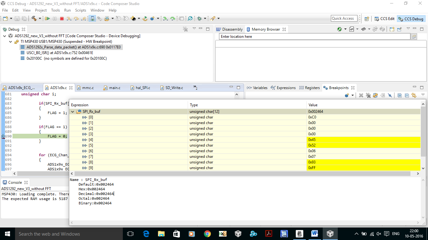
The ADS1292 is connected to a simulator and its 1st, 4th and 7th byte are known and they should be:

1st Byte - 0xC0

4th and 7th byte - 0x00

many at times I get the first byte as 0x40 and the 7th byte as 0x06 - I have not monitored the 4th byte and hence not sure if the deviation exists there or not. This is when the SPI Rx Buffer is read. while on the logic analyzer I can see that the correct byte is coming in to the MSP430F5529 from ADS1292, Given below are the screen shots:

Some observations:

  1. I have noticed that as the SCLK to ADS1292 is increased the problem is more frequent but have noticed an exception to this as well. The MSP is running at 24 MHz and SCLK for the ADS is from ACLK, I change the divider to 3 giving me a frequency of 8MHz i see that the problem remains but is less frequent.
  2. The problem is periodic, the periodicity is not like a clock work precision but its not completely random as well.
  3. Very infrequent as compared to the 7th byte the 8th byte is shown as 0x07 in the buffer.
  4. The byte being read wrongly in the buffer only after the SD card has finished writing and can be seen from the 4th picture. The SPI at the bottom is that of the micro SD card.

I request your inputs to solve this issue.

Regards

Viney Chaddha      

  • Hi Viney!

    Everytime I see anyone having problems with ADSxxxx ADC's from TI, my first question is about the configuration of the SPI module. You do not show the code and I cannot clearly see this in the scope screens, but did you configure the SPI module to latch the data on the falling edge of CLK, not on the rising? This is a mistake that is made quite often because in most cases data is latched on the rising edge. Just to make sure the problem isn't caused by this wrong bit setting.

    Dennis

  • Hi Dennis,

    UCB0CTL0 = 0x29;
    The Bit 8 is set as 0 and as per the MSP430 user guide it means the following

    0b = Data is changed on the first UCLK edge and captured on the following
    edge.
    1b = Data is captured on the first UCLK edge and changed on the following
    edge.

    Hence this is not likely to be the cause, because had it been I would expect an issue with all the bytes and not just 1 byte.

    I have also noticed that the frequency of data corruption is also depending on the type of card used - I don't know why is that happening because the two SPI are mutually exclusive (I may be wrong in saying that, but that what I think). If I use a Strontium 4 GB class 6 card it behaves differently to the SanDisk 8GB Class 10 card.

    Regards
    Viney Chaddha
  • An incorrect SPI mode (CPOL/CPHA) wouldn't necessarily (visibly) affect all bytes, since what you're reading is transitional states -- rise/fall times, pin capacitance and the like.

    When faced with mysterious SPI failures and/or indecipherable spec sheet descriptions, I usually fall back on ("last refuge of scoundrels"):

    1) Try all the SPI modes in turn -- there are only 4 of them.

    2) Slow down the SPI until something changes, or at least until it's so slow it get silly.

    These of course aren't a cure, but rather a diagnosis path.

    My experience with SD cards is that they're (a) all different, at least in the corner cases, and (b) all finicky.

  • Bruce,
    I have tried ICB0CTL0 =0xA9 but that stopped the SPI communication with the ADS all together. Have not tried the others 2 since the clock is low as per the ADS datasheet and the other 2 modes would meant that the clock is high.
    Regards
    Viney Chaddha
  • I have some problem with ADS1292 interface to MSP430F5659 controller. I am reading same value on any change in input value. What could be the reason? System runs @4Mhz and i am using ACLK for SPI, which i believe 1Mhz as per setting, but please clarify is it correct or wrong?
    UCB0CTL0 |= UCMST+UCSYNC+UCMSB;
    UCB0CTL1 |= UCSSEL__ACLK; // ACLK
    UCB0BR0 = 24; // 1 MHz
    UCB0BR1 = 0; //
    I have used this clock speed for register read/write and i have used same BR is used for Data read.
    Any thing i am missing here for clock setting?
    Any suggestion please share.

    Nitesh
  • Nitesh,

    You need to first set the UCB0CTL1  bit 0 to 1 before making any change to UCB0CTLx

    UCB0CTL1 |= UCSWRST

    UCB0CTL0 |= UCMST+UCSYNC+UCMSB;

    UCB0CTL1 |= UCSSEL__ACLK; // ACLK

    UCB0BR0 = 24; // 1 MHz

    UCB0BR1 = 0; //

    UCB0CTL1 &= ~UCSWRST


    You need to add the two lines highlighted in green.

    If the UCB0TL1 bit 0 is not set to 1 the changes can not be made and hence the change would not be registered and this bit after the change the bit needs to be set back to 0.

    What is the clock source for the ADS1292, internal or external, if external then @ what speed, While writing the registers there is a limit on SCLK speed but @1MHz the SCLK speed should be ok for register read/Write even if you consider 512 kHz for the internl clock.

    Moreover the MCLK speed is 4 MHz or 24 MHz, is the @4MHz a typo or you want to say the system runs at 4 MHz,

    "System runs @4Mhz and i am using ACLK for SPI,"

    In case the system speed is 24MHz then the ACLK with the divisor as 24 would run at 1 MHz.

    Regards

    Viney Chaddha

  • Hi Viney,

    Thanks for the reply. i am able to read the ADC count from ADS1292 channel 2 using 1Mhz SPI clock. ADS1292 has internal clock of 500KHz and sampling @ 500SPS.

    My only problem is i am seeing some drift in my ADC count.

    Here is our formula for calculating the ADC converted data for positive range.

                                         Voltage measured Value  =  Vref (2.42v)/ (2^23-1) * ADC Count (23 bit considered ignoring MSB 24bit if set)

    For Ex.

                    0.8v  input value, measured count  0x23EE91 after calculation measured voltage is – 0.67v while expected value was 0x2A5065 counts

    0.4v  input value, measured count 0x11CbD4  after calculation measured voltage is – 0.336v while expected value was 0x152832 counts


    And we are seeing constant linear drop in measured value.


    I would appreciate you, if you can help in solving this issue.


    Thanks,

    Nitesh 

  • Nitesh,
    Have you checked the test signal and the offset? Can you send the screen shot of the input signal, (may be you could plot it and post)
    Regards
    Viney Chaddha
  • Hi Viney,

    Thanks,

    I have done few experiments on channel 2 where we are giving the differential input which was suggested by our direct TI focal person.

    1. Channel 2 gain set to 1.

    2. Channel 2 input shorted by setting 001, and measured offset.  Read offset value is 13E (318.668)  

    3. Channel 2 input set to MVDD for measure power supply by setting 011. Read ADC count value is 13E (318.588). This value is almost equal to the offset value, instead of VDD/4 (3.3/4 = 0.825 v)

    i felt MVDD differential input is almost zero.

    This was not helped us. Will try as per your input and i will let you know the observations.

    Thanks,

    Nitesh

**Attention** This is a public forum