Other Parts Discussed in Thread: MSP430G2553
Dear All
i am trying to learn msp430g2553 i have a basic question ,
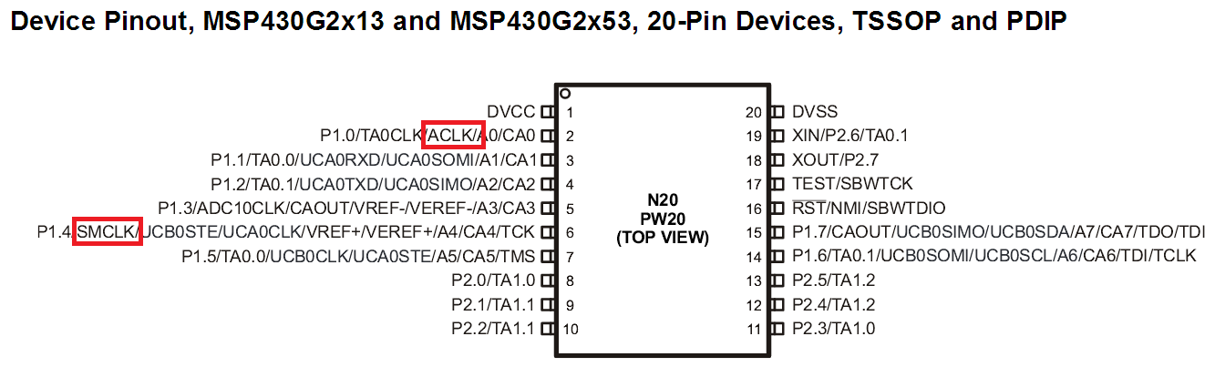
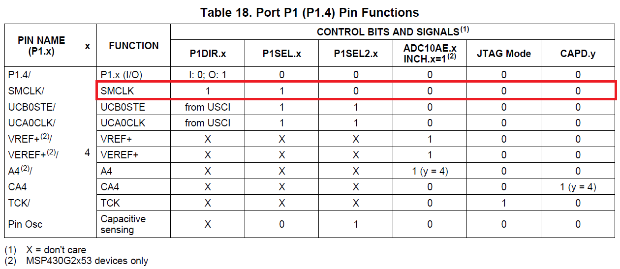
how to route the internal clock generated to an output pin for testing the frequency
Other Parts Discussed in Thread: MSP430G2553
Dear All
i am trying to learn msp430g2553 i have a basic question ,
how to route the internal clock generated to an output pin for testing the frequency
**Attention** This is a public forum