This thread has been locked.

If you have a related question, please click the "Ask a related question" button in the top right corner. The newly created question will be automatically linked to this question.

MSP432 ADC14 and DMA Usage - Destination address issues

Other Parts Discussed in Thread: BOOSTXL-EDUMKII

Jace, thank you for this threat to talk about DMA and ADC.

Mi problem begin once I use : " MAP_ADC14_configureMultiSequenceMode(ADC_MEM0, ADC_MEM1,true);" to obtain analog values  constantly and store them in ADC_MEM0 and ADCMEM1, i have modified the DMA configuration to increase the source direction "ADC_MEM0" 32 bits, but my destination address does not get filled, their values remain in 0, I need to use ping pong mode for DMA and repeat mode for ADC14, I have found examples of DMA and ADC with a SequenceMode in "not repeat mode". In your example I see that you use one DMA channel for one ADC source, in that case I will be able to use only 4 ADC sources because there are only 4 DMA_INTx_IRQHandler(if i am wrong, please, tell me). I beleave that is possible to use only one DMA channel to get information from multiple ADC sources, but I tried to do it but does no work.

#include "msp.h"
#include <driverlib.h>
#include <grlib.h>
#include <stdio.h>
#include <string.h>
#include <arm_math.h>
#include "arm_const_structs.h"


#define TEST_LENGTH_SAMPLES 512
#define SAMPLE_LENGTH 512

/* ------------------------------------------------------------------
* Global variables for FFT Bin Example
* ------------------------------------------------------------------- */
volatile long BUF_32;
volatile short m=0;

/* Graphic library context */
#define SMCLK_FREQUENCY     48000000
#define SAMPLE_FREQUENCY    600000


/* DMA Control Table */
#ifdef ewarm
#pragma data_alignment=256
#else
#pragma DATA_ALIGN(controlTable, 256)
#endif
uint8_t controlTable[256];


/* Processing buffers*/
float hann[SAMPLE_LENGTH];
int32_t data_array1[SAMPLE_LENGTH];
int32_t data_array2[SAMPLE_LENGTH];
int32_t data_array3[SAMPLE_LENGTH];
int32_t data_array4[SAMPLE_LENGTH];
int16_t salida[SAMPLE_LENGTH];

volatile int switch_data = 0;

uint32_t color = 0;
volatile uint16_t * res[2];

/* Timer_A PWM Configuration Parameter */
Timer_A_PWMConfig pwmConfig =
{
        TIMER_A_CLOCKSOURCE_SMCLK,
        TIMER_A_CLOCKSOURCE_DIVIDER_1,
        (SMCLK_FREQUENCY/SAMPLE_FREQUENCY),
        TIMER_A_CAPTURECOMPARE_REGISTER_1,
        TIMER_A_OUTPUTMODE_SET_RESET,
        (SMCLK_FREQUENCY/SAMPLE_FREQUENCY)/2
};

void main(void)
{
    /* Halting WDT and disabling master interrupts */
    MAP_WDT_A_holdTimer();
    MAP_Interrupt_disableMaster();

    /* Initializes Clock System */
    MAP_CS_setDCOCenteredFrequency(CS_DCO_FREQUENCY_48);
    MAP_CS_initClockSignal(CS_MCLK, CS_DCOCLK_SELECT, CS_CLOCK_DIVIDER_1 );
    MAP_CS_initClockSignal(CS_HSMCLK, CS_DCOCLK_SELECT, CS_CLOCK_DIVIDER_1 );
    MAP_CS_initClockSignal(CS_SMCLK, CS_DCOCLK_SELECT, CS_CLOCK_DIVIDER_1 );
    MAP_CS_initClockSignal(CS_ACLK, CS_REFOCLK_SELECT, CS_CLOCK_DIVIDER_1);

    /*---------------------------------------------------------------------------------------------------------*/
        // Configuracion de los puertos UART
        P1SEL0 |= BIT2 | BIT3;                  	// set 2-UART pin as second function
        __enable_interrupt();
        NVIC->ISER[0] = 1 << ((EUSCIA0_IRQn) & 31); // Enable eUSCIA0 interrupt in NVIC module

        // Configuracion de UART
        UCA0CTLW0 |= UCSWRST;
        UCA0CTLW0 |= UCSSEL__SMCLK;             // Pone eUSCI en reseteo
        UCA0BR0 = 26;                           // 48000000/16/9600
        UCA0MCTLW = 0x1000 | 0x0020 | UCOS16;

        UCA0BR1 = 0;
        UCA0CTLW0 &= ~UCSWRST;                  // Inicializa eUSCI
        UCA0IE |= UCRXIE;                       // habilita la interrupcion USCI_A0 RX
    /*---------------------------------------------------------------------------------------------------------*/

    /* Configuring Timer_A to have a period of approximately 500ms and
     * an initial duty cycle of 10% of that (3200 ticks)  */
    Timer_A_generatePWM(TIMER_A0_BASE, &pwmConfig);

    /*--------------------------------------------------------------------------------------------------*/
        /* Initializing ADC (MCLK/1/1) */
        ADC14_enableModule();
        ADC14_initModule(ADC_CLOCKSOURCE_MCLK, ADC_PREDIVIDER_1, ADC_DIVIDER_1, 0);

        ADC14_setSampleHoldTrigger(ADC_TRIGGER_SOURCE1, false);
    /* Configuring GPIOs (4.3 A10)*/
        MAP_GPIO_setAsPeripheralModuleFunctionInputPin(GPIO_PORT_P5, GPIO_PIN5 | GPIO_PIN4 ,GPIO_TERTIARY_MODULE_FUNCTION);
    /* Configuring ADC Memory */
//      ADC14_enableSampleTimer (ADC_AUTOMATIC_ITERATION);
      ADC14_configureSingleSampleMode(ADC_MEM0, true);

//      ADC14_configureMultiSequenceMode (ADC_MEM0, ADC_MEM1,true);
      ADC14_configureConversionMemory(ADC_MEM0, ADC_VREFPOS_AVCC_VREFNEG_VSS,ADC_INPUT_A0, false);
      ADC14_configureConversionMemory(ADC_MEM1, ADC_VREFPOS_AVCC_VREFNEG_VSS,ADC_INPUT_A1, false);
      ADC14_setResolution (ADC_12BIT);
        /* Set ADC result format to signed binary */
    //  ADC14_setResultFormat(ADC_SIGNED_BINARY);
    /*--------------------------------------------------------------------------------------------------*/
    /* Configuring DMA module */
    DMA_enableModule();
    DMA_setControlBase(controlTable);


    DMA_disableChannelAttribute(DMA_CH7_ADC14 ,
                                 UDMA_ATTR_ALTSELECT | UDMA_ATTR_USEBURST |
                                 UDMA_ATTR_HIGH_PRIORITY |
                                 UDMA_ATTR_REQMASK);

    /* Setting Control Indexes. In this case we will set the source of the
     * DMA transfer to ADC14 Memory 0
     *  and the destination to the
     * destination data array. */
    MAP_DMA_setChannelControl(UDMA_PRI_SELECT | DMA_CH7_ADC14 ,
        UDMA_SIZE_32 | UDMA_SRC_INC_32 | UDMA_DST_INC_32 | UDMA_ARB_2);
    MAP_DMA_setChannelTransfer(UDMA_PRI_SELECT | DMA_CH7_ADC14 ,
        UDMA_MODE_PINGPONG, (void*) &ADC14->MEM[0],
        data_array1, SAMPLE_LENGTH);

    MAP_DMA_setChannelControl(UDMA_ALT_SELECT | DMA_CH7_ADC14 ,
        UDMA_SIZE_32 | UDMA_SRC_INC_32 | UDMA_DST_INC_32 | UDMA_ARB_2);
    MAP_DMA_setChannelTransfer(UDMA_ALT_SELECT | DMA_CH7_ADC14 ,
        UDMA_MODE_PINGPONG, (void*) &ADC14->MEM[0],
        data_array2, SAMPLE_LENGTH);

    /* Assigning/Enabling Interrupts */
    MAP_DMA_assignInterrupt(DMA_INT1, 7);
    MAP_Interrupt_enableInterrupt(INT_DMA_INT1);
    MAP_DMA_assignChannel(DMA_CH7_ADC14);
    MAP_DMA_clearInterruptFlag(7);
    MAP_Interrupt_enableMaster();

    /* Now that the DMA is primed and setup, enabling the channels. The ADC14
     * hardware should take over and transfer/receive all bytes */
    MAP_DMA_enableChannel(7);
    MAP_ADC14_enableConversion();

    while(1)
    {
        MAP_PCM_gotoLPM0();

        int i = 0;
        int j = 0;
        /* Store data on "salida[]" */
        if (switch_data & 1)
        {
            for (i=0; i<512; i++)
            {
                salida[i] = (int16_t)(data_array1[i]);
            }
        }
        else
        {
            for (i=0; i<512; i++)
            {
                salida[i] = (int16_t)(data_array2[i]);
            }
        }
/*--------------------------------------------------------------------------------------------------------------------------*/
        /* Enviando datos a traves de UART */

        for (j = 25; j <= 512-2; j+=2)
        {
            BUF_32= salida[j+1];
            BUF_32= (BUF_32<<12)|salida[j];
            while(!(UCA0IFG&UCTXIFG)); UCA0TXBUF = (BUF_32 & 0x000000FF);
            while(!(UCA0IFG&UCTXIFG)); UCA0TXBUF = (BUF_32 & 0x0000FF00)>>8;
            while(!(UCA0IFG&UCTXIFG)); UCA0TXBUF = (BUF_32 & 0x00FF0000)>>16;
        }
/*--------------------------------------------------------------------------------------------------------------------------*/
/*--------------------------------------------------------------------------------------------------------------------------*/
    }
}

/* Completion interrupt for ADC14 MEM0 */
void DMA_INT1_IRQHandler(void)
{
    /* Switch between primary and alternate bufferes with DMA's PingPong mode */
    if (DMA_getChannelAttribute(7) & UDMA_ATTR_ALTSELECT)
    {
        DMA_setChannelControl(UDMA_PRI_SELECT | DMA_CH7_ADC14 ,
            UDMA_SIZE_32 | UDMA_SRC_INC_32 | UDMA_DST_INC_32 | UDMA_ARB_2);
        DMA_setChannelTransfer(UDMA_PRI_SELECT | DMA_CH7_ADC14 ,
            UDMA_MODE_PINGPONG, (void*) &ADC14->MEM[0],
            data_array1, SAMPLE_LENGTH);

        switch_data = 1;
    }
    else
    {
        DMA_setChannelControl(UDMA_ALT_SELECT | DMA_CH7_ADC14 ,
            UDMA_SIZE_32 | UDMA_SRC_INC_32 | UDMA_DST_INC_32 | UDMA_ARB_2);
        DMA_setChannelTransfer(UDMA_ALT_SELECT | DMA_CH7_ADC14 ,
            UDMA_MODE_PINGPONG, (void*) &ADC14->MEM[0],
            data_array2, SAMPLE_LENGTH);

        switch_data = 0;
    }
}
void EUSCIA0_IRQHandler(void)
{
   if (UCA0IFG & UCRXIFG)
    {
    }
}

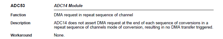
If I change "UDMA_ARB_x" to "1" it still does not work, i got the same problem, destination array does not get filled. How can I use one channel to transfer information from multiple ADC sources??

Thank you!!!!

  • Hi Josue,

    I'm looking into the matter, please allow me some time to review your code and run a few tests.

    Thanks,

    David
  • Thank you DavidL, one more question :v
    Is DMA_CH7_ADC14 the only channel to transfer data from ADC_MEM_x to a memory location?? I tried changing it but does not work with other DMA channel(in the same code above), also the problem of multichannel ADC and DMA persist. Thanks again!!!!!!!!!!!!!!
  • Hi Josue,

     Yes the DMA_CH7_ADC14 is the one mapped to the ADC.

    And I'm still working on your code.

      Thanks for your patience.

        David

  • Hi Josue,

    Which MSP432 Launchpad version are you using?? RED (Silicon Rev C) or BLACK (Silicon Rev B)?? ( www.ti.com/.../msp-exp432p401r)
    Thanks,

    David

  • The Black one (Silicon Rev B)
  • Hi Josue,

     This behavior is related to the Errata ADC53 and it got corrected on Rev C.

    I only made a couple of changes to your code and I got it to work with the Rev C.

    Best regards,

      David

  • Hi DavilL, thanks you very much, so, the problem can not be solved on the Black silicon board??, where I can find the errata documentation, and what kind of changes do you made to the code??? the changes whre on the ADC configuration?? or DMA configuration??
    both of them??, I thought that it was a problem of the DriverLib.
    Thanks again!!!.
  • Hi Josue!

    The Erratasheet can be found here.

    You can find the link on the product webpage of the MSP432P401R:

    But it looks like the Erratasheet has lost almost all of it's content (issues fixed in silicon rev. C) - there are only four issues left and the one mentioned by David is no longer present:

    Dennis

  • hi, Guys

    So is this confirmed  the DMA and ADC14 does not work together on the black version (version B) board? how does it impact the ability of the board to do high speed (hundreds of kHz) ADC acquisition and transfer the data to PC using UART. 

    best, 

  • Hi David,

    I am new to working with TI microcontrollers and I am trying to get the microphoneFFT example to work properly (it is nearly identical to Josue's code). When I run the code, I get two DMA interrupts and then the ADC fails to trigger further interrupts. I have an updated CMSIS DSP library and downloaded new driverlib files. CCS is also up to date and the MSP432 is running with the new SimpleLink SDK.

    Some of these questions are rather simple, but I could not find answers online so I hope you can answer a few questions I have:

    • Are all Red MSP432's Rev. C? I am using the MSP-EXP432P401R Rev 2.1
    • Is Rev C a software or hardware update from Rev. B?
    • How did you migrate the code to Rev. C?

    Best,

    Jeff

  • Jeff,
    What you are describing would suggest that the DMA is not being properly reconfigured. The first two DMA interrupts would be for the primary and then the alternate. Ideally what would happen is that during the ping-pong the primary would be updated while the alternate is collecting and the alternate would update when the primary is collecting.

    I believe all red boards are Revision C, and more specifically, Revision 2.1 is revision C. You should be able to verify this on the actual silicon in both the revision marking as well as that the silicon is marked MSP432P401R and not XMS432P401R. Please note that there are some red launchpads that have silicon marked XMS but are still revision C silicon.

    Revision C is a hardware update and addition to the hardware the ROM firmware has been updated from revision B. This document www.ti.com/.../slaa700a.pdf has been provided to describe migration.

    Please let me know if you have any specific questions or issues.

    Chris
  • Hi Chris,

    Thanks for the response. I believe my software and hardware are both up to date.

    Unfortunately the ping-pong sequence does not continue after the first two interrupts. I'm not sure why the DMA is not properly configured because I am running a lightly modified version of the "BOOSTXL-EDUMKII_MicrophoneFFT" example provided by TI. This shouldn't affect things, but I am not using the BOOSTXL-EDUMKII booster pack. Instead, I have attached the ADC pin to a hall effect sensor. 

    Best,

    Jeff

    /* --COPYRIGHT--,BSD
     * Copyright (c) 2015, Texas Instruments Incorporated
     * All rights reserved.
     *
     * Redistribution and use in source and binary forms, with or without
     * modification, are permitted provided that the following conditions
     * are met:
     *
     * *  Redistributions of source code must retain the above copyright
     *    notice, this list of conditions and the following disclaimer.
     *
     * *  Redistributions in binary form must reproduce the above copyright
     *    notice, this list of conditions and the following disclaimer in the
     *    documentation and/or other materials provided with the distribution.
     *
     * *  Neither the name of Texas Instruments Incorporated nor the names of
     *    its contributors may be used to endorse or promote products derived
     *    from this software without specific prior written permission.
     *
     * THIS SOFTWARE IS PROVIDED BY THE COPYRIGHT HOLDERS AND CONTRIBUTORS "AS IS"
     * AND ANY EXPRESS OR IMPLIED WARRANTIES, INCLUDING, BUT NOT LIMITED TO,
     * THE IMPLIED WARRANTIES OF MERCHANTABILITY AND FITNESS FOR A PARTICULAR
     * PURPOSE ARE DISCLAIMED. IN NO EVENT SHALL THE COPYRIGHT OWNER OR
     * CONTRIBUTORS BE LIABLE FOR ANY DIRECT, INDIRECT, INCIDENTAL, SPECIAL,
     * EXEMPLARY, OR CONSEQUENTIAL DAMAGES (INCLUDING, BUT NOT LIMITED TO,
     * PROCUREMENT OF SUBSTITUTE GOODS OR SERVICES; LOSS OF USE, DATA, OR PROFITS;
     * OR BUSINESS INTERRUPTION) HOWEVER CAUSED AND ON ANY THEORY OF LIABILITY,
     * WHETHER IN CONTRACT, STRICT LIABILITY, OR TORT (INCLUDING NEGLIGENCE OR
     * OTHERWISE) ARISING IN ANY WAY OUT OF THE USE OF THIS SOFTWARE,
     * EVEN IF ADVISED OF THE POSSIBILITY OF SUCH DAMAGE.
     * --/COPYRIGHT--*/
    //****************************************************************************
    //
    // main.c - MSP-EXP432P401R + Educational Boosterpack MkII - Microphone FFT
    //
    //          CMSIS DSP Software Library is used to perform 512-point FFT on
    //          the audio samples collected with MSP432's ADC14 from the Education
    //          Boosterpack's onboard microhpone. The resulting frequency bin data
    //          is displayed on the BoosterPack's 128x128 LCD.
    //
    //****************************************************************************
    
    #include "msp.h"
    #include <driverlib.h>
    #include <stdio.h>
    #include <arm_math.h>
    #include "arm_const_structs.h"
    
    
    #define TEST_LENGTH_SAMPLES 512
    #define SAMPLE_LENGTH 512
    #define ARM_MATH_DSP
    
    /* ------------------------------------------------------------------
    * Global variables for FFT Bin Example
    * ------------------------------------------------------------------- */
    uint32_t fftSize = SAMPLE_LENGTH;
    uint32_t ifftFlag = 0;
    uint32_t doBitReverse = 1;
    volatile arm_status status;
    
    /* Graphic library context */
    //Graphics_Context g_sContext;
    
    #define SMCLK_FREQUENCY     48000000
    #define SAMPLE_FREQUENCY    8000
    
    
    /* DMA Control Table */
    #ifdef ewarm
    #pragma data_alignment=256
    #else
    #pragma DATA_ALIGN(controlTable, 256)
    #endif
    uint8_t controlTable[256];
    
    
    /* FFT data/processing buffers*/
    float hann[SAMPLE_LENGTH];
    int16_t data_array1[SAMPLE_LENGTH];
    int16_t data_array2[SAMPLE_LENGTH];
    int16_t data_input[SAMPLE_LENGTH*2];
    int16_t data_output[SAMPLE_LENGTH];
    
    volatile int switch_data = 0;
    
    uint32_t color = 0;
    
    /* Timer_A PWM Configuration Parameter */
    Timer_A_PWMConfig pwmConfig =
    {
            TIMER_A_CLOCKSOURCE_SMCLK,
            TIMER_A_CLOCKSOURCE_DIVIDER_1,
            (SMCLK_FREQUENCY/SAMPLE_FREQUENCY),
            TIMER_A_CAPTURECOMPARE_REGISTER_1,
            TIMER_A_OUTPUTMODE_SET_RESET,
            (SMCLK_FREQUENCY/SAMPLE_FREQUENCY)/2
    };
    
    void main(void)
    {
        /* Halting WDT and disabling master interrupts */
        MAP_WDT_A_holdTimer();
        MAP_Interrupt_disableMaster();
    
        /* Set to Vcore1 */
        MAP_PCM_setCoreVoltageLevel(PCM_VCORE1);
    
        /* Set to use DCDC */
        MAP_PCM_setPowerState(PCM_AM_DCDC_VCORE1);
    
        /* Set wait state */
        MAP_FlashCtl_setWaitState(FLASH_BANK0, 2);
        MAP_FlashCtl_setWaitState(FLASH_BANK1, 2);
    
        /* Initializes Clock System */
        MAP_CS_setDCOCenteredFrequency(CS_DCO_FREQUENCY_48);
        MAP_CS_initClockSignal(CS_MCLK, CS_DCOCLK_SELECT, CS_CLOCK_DIVIDER_1 );
        MAP_CS_initClockSignal(CS_HSMCLK, CS_DCOCLK_SELECT, CS_CLOCK_DIVIDER_1 );
        MAP_CS_initClockSignal(CS_SMCLK, CS_DCOCLK_SELECT, CS_CLOCK_DIVIDER_1 );
        MAP_CS_initClockSignal(CS_ACLK, CS_REFOCLK_SELECT, CS_CLOCK_DIVIDER_1);
    
        /* Terminating all remaining pins to minimize power consumption. This is
            done by register accesses for simplicity and to minimize branching API
            calls */
        MAP_GPIO_setAsOutputPin(GPIO_PORT_P1, PIN_ALL16);
        MAP_GPIO_setAsOutputPin(GPIO_PORT_P2, PIN_ALL16);
        MAP_GPIO_setAsOutputPin(GPIO_PORT_PB, PIN_ALL16);
        MAP_GPIO_setAsOutputPin(GPIO_PORT_PC, PIN_ALL16);
        MAP_GPIO_setAsOutputPin(GPIO_PORT_PD, PIN_ALL16);
        MAP_GPIO_setAsOutputPin(GPIO_PORT_PE, PIN_ALL16);
        MAP_GPIO_setOutputLowOnPin(GPIO_PORT_P2, PIN_ALL16);
        MAP_GPIO_setOutputLowOnPin(GPIO_PORT_PB, PIN_ALL16);
        MAP_GPIO_setOutputLowOnPin(GPIO_PORT_PC, PIN_ALL16);
        MAP_GPIO_setOutputLowOnPin(GPIO_PORT_PD, PIN_ALL16);
        MAP_GPIO_setOutputLowOnPin(GPIO_PORT_PE, PIN_ALL16);


        // Initialize Hann Window
        int n;
        for (n = 0; n < SAMPLE_LENGTH; n++)
        {
            hann[n] = 0.5 - 0.5 * cosf((2*PI*n)/(SAMPLE_LENGTH-1));
        }
    
        /* Configuring Timer_A to have a period of approximately 500ms and
         * an initial duty cycle of 10% of that (3200 ticks)  */
        Timer_A_generatePWM(TIMER_A0_BASE, &pwmConfig);
    
        /* Initializing ADC (MCLK/1/1) */
        ADC14_enableModule();
        ADC14_initModule(ADC_CLOCKSOURCE_MCLK, ADC_PREDIVIDER_1, ADC_DIVIDER_1, 0);
    
        ADC14_setSampleHoldTrigger(ADC_TRIGGER_SOURCE1, false);
    
        /* Configuring GPIOs (4.3 A10) */
        GPIO_setAsPeripheralModuleFunctionInputPin(GPIO_PORT_P4, GPIO_PIN3,
        GPIO_TERTIARY_MODULE_FUNCTION);
    
        /* Configuring ADC Memory */
        ADC14_configureSingleSampleMode(ADC_MEM0, true);
        ADC14_configureConversionMemory(ADC_MEM0, ADC_VREFPOS_AVCC_VREFNEG_VSS,
        ADC_INPUT_A10, false);
    
        /* Set ADC result format to signed binary */
        ADC14_setResultFormat(ADC_SIGNED_BINARY);
    
        /* Configuring DMA module */
        DMA_enableModule();
        DMA_setControlBase(controlTable);
    
    
        DMA_disableChannelAttribute(DMA_CH7_ADC14,
                                     UDMA_ATTR_ALTSELECT | UDMA_ATTR_USEBURST |
                                     UDMA_ATTR_HIGH_PRIORITY |
                                     UDMA_ATTR_REQMASK);
    
    
        /* Setting Control Indexes. In this case we will set the source of the
         * DMA transfer to ADC14 Memory 0
         *  and the destination to the
         * destination data array. */
        MAP_DMA_setChannelControl(UDMA_PRI_SELECT | DMA_CH7_ADC14,
            UDMA_SIZE_16 | UDMA_SRC_INC_NONE | UDMA_DST_INC_16 | UDMA_ARB_1);
        MAP_DMA_setChannelTransfer(UDMA_PRI_SELECT | DMA_CH7_ADC14,
            UDMA_MODE_PINGPONG, (void*) &ADC14->MEM[0],
            data_array1, SAMPLE_LENGTH);
    
        MAP_DMA_setChannelControl(UDMA_ALT_SELECT | DMA_CH7_ADC14,
            UDMA_SIZE_16 | UDMA_SRC_INC_NONE | UDMA_DST_INC_16 | UDMA_ARB_1);
        MAP_DMA_setChannelTransfer(UDMA_ALT_SELECT | DMA_CH7_ADC14,
            UDMA_MODE_PINGPONG, (void*) &ADC14->MEM[0],
            data_array2, SAMPLE_LENGTH);
    
        /* Assigning/Enabling Interrupts */
        MAP_DMA_assignInterrupt(DMA_INT1, 7);                                           // Interrupt 1, Channel 7
        MAP_Interrupt_enableInterrupt(INT_DMA_INT1);
        MAP_DMA_assignChannel(DMA_CH7_ADC14);
        MAP_DMA_clearInterruptFlag(7);
        MAP_Interrupt_enableMaster();
    
        /* Now that the DMA is primed and setup, enabling the channels. The ADC14
         * hardware should take over and transfer/receive all bytes */
        MAP_DMA_enableChannel(7);
        MAP_ADC14_enableConversion();
    
        while(1)
        {
            MAP_PCM_gotoLPM0();
    
            int i = 0;
    
            /* Computer real FFT using the completed data buffer */
            if (switch_data & 1)
            {
                for (i=0; i<512; i++)
                {
                    data_array1[i] = (int16_t)(hann[i]*data_array1[i]);
                }
                arm_rfft_instance_q15 instance;
                status = arm_rfft_init_q15(&instance, fftSize, ifftFlag, doBitReverse);
    
                arm_rfft_q15(&instance, data_array1, data_input);
            }
            else
            {
                for (i=0; i<512; i++)
                {
                    data_array2[i] = (int16_t)(hann[i]*data_array2[i]);
                }
                arm_rfft_instance_q15 instance;
                status = arm_rfft_init_q15(&instance, fftSize, ifftFlag, doBitReverse);
    
                arm_rfft_q15(&instance, data_array2, data_input);
            }
    
            /* Calculate magnitude of FFT complex output */
            for (i = 0; i < 1024; i+=2)
            {
                data_output[i/2] = (int32_t)(sqrtf((data_input[i] * data_input[i]) + (data_input[i+1] * data_input[i+1])));
            }
    
            q15_t maxValue;
            uint32_t maxIndex = 0;
    
            arm_max_q15(data_output, fftSize, &maxValue, &maxIndex);
    
        }
    }
    
    
    /* Completion interrupt for ADC14 MEM0 */
    void DMA_INT1_IRQHandler(void)
    {
        printf("Interrupt\n");
    
        /* Switch between primary and alternate bufferes with DMA's PingPong mode */
        if (DMA_getChannelAttribute(7) & UDMA_ATTR_ALTSELECT)
        {
            DMA_setChannelControl(UDMA_PRI_SELECT | DMA_CH7_ADC14,
                UDMA_SIZE_16 | UDMA_SRC_INC_NONE | UDMA_DST_INC_16 | UDMA_ARB_1);
            DMA_setChannelTransfer(UDMA_PRI_SELECT | DMA_CH7_ADC14,
                UDMA_MODE_PINGPONG, (void*) &ADC14->MEM[0],
                data_array1, SAMPLE_LENGTH);
            switch_data = 1;
        }
        else
        {
            DMA_setChannelControl(UDMA_ALT_SELECT | DMA_CH7_ADC14,
                UDMA_SIZE_16 | UDMA_SRC_INC_NONE | UDMA_DST_INC_16 | UDMA_ARB_1);
            DMA_setChannelTransfer(UDMA_ALT_SELECT | DMA_CH7_ADC14,
                UDMA_MODE_PINGPONG, (void*) &ADC14->MEM[0],
                data_array2, SAMPLE_LENGTH);
            switch_data = 0;
        }
    }
    

  • I would recommend removing the printf statement and possibly changing the update to be faster with the following:

    /* Completion interrupt for ADC14 MEM0 */

    __attribute__((ramfunc))  // Requires compiler TI v15.12.1.LTS

    void DMA_INT1_IRQHandler(void)

    {

       P1->OUT |= BIT0;

       /*

        * Switch between primary and alternate bufferes with DMA's PingPong mode

        */

       if (MAP_DMA_getChannelAttribute(7) & UDMA_ATTR_ALTSELECT)

       {

    //        MAP_DMA_setChannelControl(UDMA_PRI_SELECT | DMA_CH7_ADC14,

    //         UDMA_SIZE_16 | UDMA_SRC_INC_NONE | UDMA_DST_INC_16 | UDMA_ARB_1);

    //        MAP_DMA_setChannelTransfer(UDMA_PRI_SELECT | DMA_CH7_ADC14,

    //         UDMA_MODE_PINGPONG, (void*) &ADC14->MEM[0],

    //     resultsBufferPrimary, ARRAY_LENGTH);

        MSP_EXP432P401RLP_DMAControlTable[7].control =

        (MSP_EXP432P401RLP_DMAControlTable[7].control & 0xff000000 ) |

    (((ARRAY_LENGTH)-1)<<4) | 0x03;

       }

       else

       {

    //        MAP_DMA_setChannelControl(UDMA_ALT_SELECT | DMA_CH7_ADC14,

    //         UDMA_SIZE_16 | UDMA_SRC_INC_NONE | UDMA_DST_INC_16 | UDMA_ARB_1);

    //        MAP_DMA_setChannelTransfer(UDMA_ALT_SELECT | DMA_CH7_ADC14,

    //         UDMA_MODE_PINGPONG, (void*) &ADC14->MEM[0],

    //     resultsBufferAlternate, ARRAY_LENGTH);

        MAP_Timer_A_stopTimer(TIMER_A0_BASE);

           MAP_DMA_disableChannel(7);

        MSP_EXP432P401RLP_DMAControlTable[15].control =

        (MSP_EXP432P401RLP_DMAControlTable[15].control & 0xff000000 ) |

    (((ARRAY_LENGTH)-1)<<4) | 0x03;

       }

       P1->OUT &= ~BIT0;

    }

    /*
     * -------------------------------------------
     *    MSP432 DriverLib - v3_10_00_09 
     * -------------------------------------------
     *
     * --COPYRIGHT--,BSD,BSD
     * Copyright (c) 2014, Texas Instruments Incorporated
     * All rights reserved.
     *
     * Redistribution and use in source and binary forms, with or without
     * modification, are permitted provided that the following conditions
     * are met:
     *
     * *  Redistributions of source code must retain the above copyright
     *    notice, this list of conditions and the following disclaimer.
     *
     * *  Redistributions in binary form must reproduce the above copyright
     *    notice, this list of conditions and the following disclaimer in the
     *    documentation and/or other materials provided with the distribution.
     *
     * *  Neither the name of Texas Instruments Incorporated nor the names of
     *    its contributors may be used to endorse or promote products derived
     *    from this software without specific prior written permission.
     *
     * THIS SOFTWARE IS PROVIDED BY THE COPYRIGHT HOLDERS AND CONTRIBUTORS "AS IS"
     * AND ANY EXPRESS OR IMPLIED WARRANTIES, INCLUDING, BUT NOT LIMITED TO,
     * THE IMPLIED WARRANTIES OF MERCHANTABILITY AND FITNESS FOR A PARTICULAR
     * PURPOSE ARE DISCLAIMED. IN NO EVENT SHALL THE COPYRIGHT OWNER OR
     * CONTRIBUTORS BE LIABLE FOR ANY DIRECT, INDIRECT, INCIDENTAL, SPECIAL,
     * EXEMPLARY, OR CONSEQUENTIAL DAMAGES (INCLUDING, BUT NOT LIMITED TO,
     * PROCUREMENT OF SUBSTITUTE GOODS OR SERVICES; LOSS OF USE, DATA, OR PROFITS;
     * OR BUSINESS INTERRUPTION) HOWEVER CAUSED AND ON ANY THEORY OF LIABILITY,
     * WHETHER IN CONTRACT, STRICT LIABILITY, OR TORT (INCLUDING NEGLIGENCE OR
     * OTHERWISE) ARISING IN ANY WAY OUT OF THE USE OF THIS SOFTWARE,
     * EVEN IF ADVISED OF THE POSSIBILITY OF SUCH DAMAGE.
     * --/COPYRIGHT--*/
    /*******************************************************************************
     * MSP432 ADC14 - Single Channel Repeated Sample w/ Timer_A Trigger
     *
     * Description: In this ADC14 code example, a single input channel is sampled
     * using the standard 3.3v reference. The source of the sample trigger for this
     * example is Timer_A CCR1. The ADC is setup to sample based upon the pulse
     * sample mode and the DMA moves the result into the ping-pong buffer. Timer_A,
     * CCR0 and CCR1, are configured to generate a PWM. The CCR0 value is 27 and CCR1
     * is set to 11, resulting in a PWM of 1.167us period.  The sample time is driven
     * by the ADC clock and not the PWM duty cycle.
     *
     * The PWM is started once the GPIO interrupt for P1.1 is serviced.
     *
     *                MSP432P401
     *             ------------------
     *         /|\|                  |
     *          | |                  |
     *          --|RST         P5.5  |<--- A0 (Analog Input)
     *            |                  |
     *            |            P1.1  |<--- GPIO trigger to Start conversions
     *            |                  |
     *            |            P1.0  |---> Debug port to show DMA ISR
     *            |            P2.4  |---> Debug TA0.1, ADC trigger
     *            |                  |
     *
     * Author: Timothy Logan/ C. Sterzik
     ******************************************************************************/
    /* DriverLib Includes */
    #include "driverlib.h"
    
    /* Standard Includes */
    #include <stdint.h>
    #include <stdbool.h>
    
    #define ARRAY_LENGTH	256
    
    /*
     * Timer_A Compare Configuration Parameter
     * CCR1 is used to trigger the ADC14, conversion time
     * is defined by the resolution
     * 14bit -> 16 cycles + 1 cycle (SLAU356d, 20.2.8.3)
     * 12bit -> 14 cycles + 1 cycle
     * 10bit -> 11 cycles + 1 cycle
     *  8bit ->  9 cycles + 1 cycle
     *
     *  The timer Trigger requires 2 ADC clocks for sync
     *
     *  In this example, 14-bit resolution at 24Mhz ~708ns conversion time
     *  Sample time is defined by 4+1 ADC clocks, pulse sample mode, and
     *  timer sync is 2 ADC clocks: total 24 ADC clocks or 1us
     *  Sample period is 28/24Mhz = 1.167us
     *  
     *
     */
    const Timer_A_PWMConfig timerA_PWM =
    {
        .clockSource = TIMER_A_CLOCKSOURCE_SMCLK,
        .clockSourceDivider = TIMER_A_CLOCKSOURCE_DIVIDER_1,
        .timerPeriod = 27,
        .compareRegister = TIMER_A_CAPTURECOMPARE_REGISTER_1,
        .compareOutputMode TIMER_A_OUTPUTMODE_SET_RESET,
        .dutyCycle = 11
    };
    
    /* DMA Control Table */
    #if defined(__TI_COMPILER_VERSION__)
    #pragma DATA_ALIGN(MSP_EXP432P401RLP_DMAControlTable, 1024)
    #elif defined(__IAR_SYSTEMS_ICC__)
    #pragma data_alignment=1024
    #elif defined(__GNUC__)
    __attribute__ ((aligned (1024)))
    #elif defined(__CC_ARM)
    __align(1024)
    #endif
    static DMA_ControlTable MSP_EXP432P401RLP_DMAControlTable[16];
    
    /* Statics */
    static volatile uint16_t resultsBufferPrimary[ARRAY_LENGTH];
    static volatile uint16_t resultsBufferAlternate[ARRAY_LENGTH];
    
    int main(void)
    {
        /* Halting WDT  */
        MAP_WDT_A_holdTimer();
        MAP_Interrupt_enableSleepOnIsrExit();
    
        /* Starting HFXT in non-bypass mode without a timeout. Before we start
          * we have to change VCORE to 1 to support the 48MHz frequency */
    //    MAP_PCM_setCoreVoltageLevel(PCM_VCORE1);
    //    MAP_FlashCtl_setWaitState(FLASH_BANK0, 2);
    //    MAP_FlashCtl_setWaitState(FLASH_BANK1, 2);
    
        /*
         * Revision C silicon supports wait states of 1 at 48Mhz
         */
        MAP_PCM_setCoreVoltageLevel(PCM_VCORE1);
        MAP_FlashCtl_setWaitState(FLASH_BANK0, 1);
        MAP_FlashCtl_setWaitState(FLASH_BANK1, 1);
    
        /*
         * Setting up clocks
         * MCLK = MCLK = 48MHz
         * SMCLK = MCLK/2 = 24Mhz
         * ACLK = REFO = 32Khz
         */
        MAP_CS_setDCOFrequency(48000000);
        MAP_CS_initClockSignal(CS_ACLK, CS_REFOCLK_SELECT, CS_CLOCK_DIVIDER_1);
        MAP_CS_initClockSignal(CS_SMCLK, CS_DCOCLK_SELECT, CS_CLOCK_DIVIDER_2);
        MAP_CS_initClockSignal(CS_MCLK, CS_DCOCLK_SELECT, CS_CLOCK_DIVIDER_1);
    
        /* Initializing ADC (SMCLK/1/1) */
        MAP_ADC14_enableModule();
        MAP_ADC14_initModule(ADC_CLOCKSOURCE_SMCLK, ADC_PREDIVIDER_1, ADC_DIVIDER_1,
                0);
    
        /*
         * Debug
         * Configuring P1.0 as output
         */
        MAP_GPIO_setAsOutputPin(GPIO_PORT_P1, GPIO_PIN0);
        P1OUT &= ~BIT0;
    
        /*
         * Configuring GPIOs (5.5 A0)
         */
        MAP_GPIO_setAsPeripheralModuleFunctionInputPin(GPIO_PORT_P5, GPIO_PIN5,
        GPIO_TERTIARY_MODULE_FUNCTION);
    
        /*
         * Debug: set TA0.1 as output to see ADC trigger signal
         */
        MAP_GPIO_setAsPeripheralModuleFunctionOutputPin(GPIO_PORT_P2, GPIO_PIN4,
        GPIO_PRIMARY_MODULE_FUNCTION);
    
        /*
         * Configuring P1.1 as an input and enabling interrupt, the timer is started from
         * GPIO ISR.
         */
        MAP_GPIO_setAsInputPinWithPullUpResistor(GPIO_PORT_P1, GPIO_PIN1);
        MAP_GPIO_interruptEdgeSelect(GPIO_PORT_P1,GPIO_PIN1,GPIO_HIGH_TO_LOW_TRANSITION);
        MAP_GPIO_clearInterruptFlag(GPIO_PORT_P1, GPIO_PIN1);
        MAP_GPIO_enableInterrupt(GPIO_PORT_P1, GPIO_PIN1);
    
        /*
         * Configuring ADC Memory, repeat-single-channel, A0
         */
        MAP_ADC14_configureSingleSampleMode(ADC_MEM0, true);
    
        /*
         * Configuring ADC Memory, reference, and single ended conversion
         * A0 goes to mem0, AVcc is the reference, and the conversion is
         * single-ended
         */
        MAP_ADC14_configureConversionMemory(ADC_MEM0, ADC_VREFPOS_AVCC_VREFNEG_VSS,
        ADC_INPUT_A0, false);
        /*
         * Configuring the sample trigger to be sourced from Timer_A0 CCR1 and on the
         * rising edge, default samplemode is extended (SHP=0)
         */
        MAP_ADC14_setSampleHoldTrigger(ADC_TRIGGER_SOURCE1, false);
    
        /*
         * Set SHP=1 for pulse sample mode, and set length to 4 clocks, the ADC
         * is manually triggered from the timer
         */
        MAP_ADC14_enableSampleTimer(ADC_MANUAL_ITERATION);
        MAP_ADC14_setSampleHoldTime(ADC_PULSE_WIDTH_4,ADC_PULSE_WIDTH_4);
    
        /* Enabling the interrupt when a conversion on channel 1 is complete and
         * enabling conversions */
    //    MAP_ADC14_enableInterrupt(ADC_INT0);
        MAP_ADC14_enableConversion();
    
        /* Configuring DMA module */
        MAP_DMA_enableModule();
        MAP_DMA_setControlBase(MSP_EXP432P401RLP_DMAControlTable);
    
        /*
         * Setup the DMA + ADC14 interface
         */
        MAP_DMA_disableChannelAttribute(DMA_CH7_ADC14,
                                     UDMA_ATTR_ALTSELECT | UDMA_ATTR_USEBURST |
                                     UDMA_ATTR_HIGH_PRIORITY |
                                     UDMA_ATTR_REQMASK);
    
        /*
         * Setting Control Indexes. In this case we will set the source of the
         * DMA transfer to ADC14 Memory 0 and the destination to the destination
         * data array.
         */
        MAP_DMA_setChannelControl(UDMA_PRI_SELECT | DMA_CH7_ADC14,
        		UDMA_SIZE_16 | UDMA_SRC_INC_NONE | UDMA_DST_INC_16 | UDMA_ARB_1);
        MAP_DMA_setChannelTransfer(UDMA_PRI_SELECT | DMA_CH7_ADC14,
        		UDMA_MODE_PINGPONG, (void*) &ADC14->MEM[0],
    			(void*)resultsBufferPrimary, ARRAY_LENGTH);
        MAP_DMA_setChannelControl(UDMA_ALT_SELECT | DMA_CH7_ADC14,
        		UDMA_SIZE_16 | UDMA_SRC_INC_NONE | UDMA_DST_INC_16 | UDMA_ARB_1);
        MAP_DMA_setChannelTransfer(UDMA_ALT_SELECT | DMA_CH7_ADC14,
        		UDMA_MODE_PINGPONG, (void*) &ADC14->MEM[0],
    			(void*)resultsBufferAlternate, ARRAY_LENGTH);
    
        /* Assigning/Enabling Interrupts */
        MAP_DMA_assignInterrupt(DMA_INT1, 7);
        MAP_DMA_assignChannel(DMA_CH7_ADC14);
        MAP_DMA_clearInterruptFlag(7);
    
        /* Enabling Interrupts */
        MAP_Interrupt_enableInterrupt(INT_DMA_INT1);
        MAP_Interrupt_enableInterrupt(INT_PORT1);
        MAP_Interrupt_enableMaster();
    
        /* Going to sleep */
        MAP_PCM_gotoLPM0();
        __no_operation();
    }
    
    /* Completion interrupt for ADC14 MEM0 */
    __attribute__((ramfunc))  // Requires compiler TI v15.12.1.LTS
    void DMA_INT1_IRQHandler(void)
    {
        P1->OUT |= BIT0;
        /*
         * Switch between primary and alternate bufferes with DMA's PingPong mode
         */
        if (MAP_DMA_getChannelAttribute(7) & UDMA_ATTR_ALTSELECT)
        {
    //        MAP_DMA_setChannelControl(UDMA_PRI_SELECT | DMA_CH7_ADC14,
    //        		UDMA_SIZE_16 | UDMA_SRC_INC_NONE | UDMA_DST_INC_16 | UDMA_ARB_1);
    //        MAP_DMA_setChannelTransfer(UDMA_PRI_SELECT | DMA_CH7_ADC14,
    //        		UDMA_MODE_PINGPONG, (void*) &ADC14->MEM[0],
    //    			resultsBufferPrimary, ARRAY_LENGTH);
        	MSP_EXP432P401RLP_DMAControlTable[7].control =
        			(MSP_EXP432P401RLP_DMAControlTable[7].control & 0xff000000 ) |
    				(((ARRAY_LENGTH)-1)<<4) | 0x03;
        }
        else
        {
    //        MAP_DMA_setChannelControl(UDMA_ALT_SELECT | DMA_CH7_ADC14,
    //        		UDMA_SIZE_16 | UDMA_SRC_INC_NONE | UDMA_DST_INC_16 | UDMA_ARB_1);
    //        MAP_DMA_setChannelTransfer(UDMA_ALT_SELECT | DMA_CH7_ADC14,
    //        		UDMA_MODE_PINGPONG, (void*) &ADC14->MEM[0],
    //    			resultsBufferAlternate, ARRAY_LENGTH);
        	MAP_Timer_A_stopTimer(TIMER_A0_BASE);
            MAP_DMA_disableChannel(7);
        	MSP_EXP432P401RLP_DMAControlTable[15].control =
        			(MSP_EXP432P401RLP_DMAControlTable[15].control & 0xff000000 ) |
    				(((ARRAY_LENGTH)-1)<<4) | 0x03;
        }
        P1->OUT &= ~BIT0;
    }
    
    void PORT1_IRQHandler(void)
    {
        P1->OUT |= BIT0;
        P1IFG &= ~BIT1;
        MAP_DMA_enableChannel(7);
        MAP_Timer_A_generatePWM(TIMER_A0_BASE, &timerA_PWM);
        P1->OUT &= ~BIT0;
    }
    

    Regrets for the delay,

    Chris

**Attention** This is a public forum