Other Parts Discussed in Thread: ENERGYTRACE
Good afternoon,
my code sleeps and wakes up upon a rising edge interrupt on P3.3 pin :)
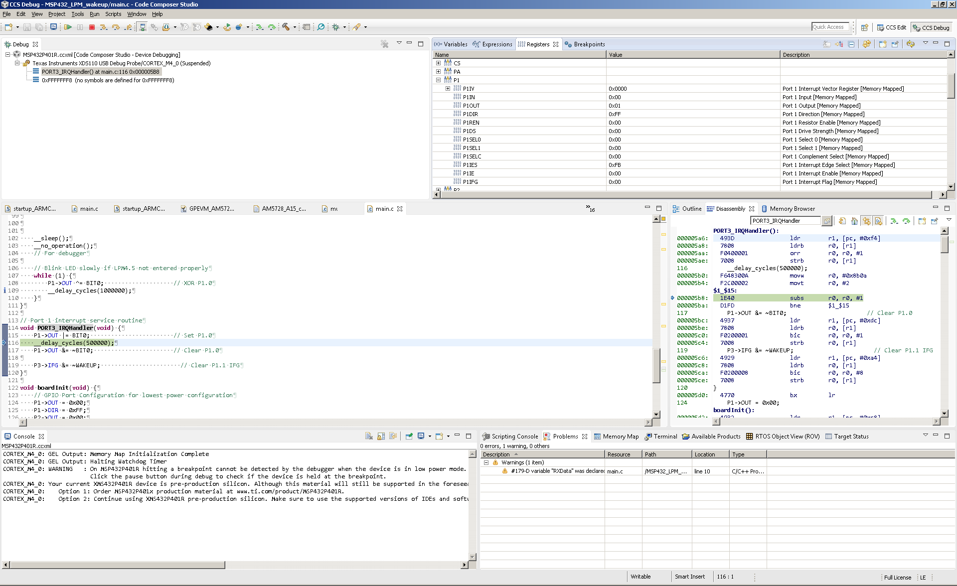
The code works when debugged. However, it does NOT when unplugged and I press the reset pin. I have seen similar E2E threads but was not able to apply the solutions there to success. BTW, just ignore the SPI section.
#include "msp.h"
#include <stdint.h>

#define WAKEUP		BIT3
#define SPI_CS 		BIT3
#define BLUE_LED 	BIT2
#define GREEN_LED	BIT1
#define RED_LED		BIT0

static uint8_t RXData[100] = { 0 };
volatile uint8_t idx_RXData = 0;

void send_cmd_to_spi(uint8_t, uint8_t);

void boardInit(void);

int main(void) {
	WDT_A->CTL = WDT_A_CTL_PW |             // Stop WDT
			WDT_A_CTL_HOLD;

	__delay_cycles(1000000);

	// Initialize GPIO and clocks
	boardInit();

	// Configuring P1 as output and P1.1 (switch) as input with pull-up resistor
	P3->SEL0 &= ~WAKEUP;
	P3->DIR &= ~WAKEUP;
	P3->OUT &= ~WAKEUP;
	P3->REN |= WAKEUP;
	P3->IFG &= ~WAKEUP;
	P3->IES &= ~WAKEUP; /*!< Port Interrupt Edge Select */
	P3->IE |= WAKEUP;

	// Turn off PSS high-side supervisors
	PSS->KEY = PSS_KEY_KEY_VAL;
	PSS->CTL0 |= PSS_CTL0_SVSMHOFF;
	PSS->KEY = 0;

	// Enable all SRAM bank retentions prior to going to LPM3 (Deep-sleep)
	SYSCTL->SRAM_BANKRET |= (SYSCTL_SRAM_BANKRET_BNK1_RET
			| SYSCTL_SRAM_BANKRET_BNK2_RET | SYSCTL_SRAM_BANKRET_BNK3_RET
			| SYSCTL_SRAM_BANKRET_BNK4_RET | SYSCTL_SRAM_BANKRET_BNK5_RET
			| SYSCTL_SRAM_BANKRET_BNK6_RET | SYSCTL_SRAM_BANKRET_BNK7_RET);

	// Enable global interrupt
	__enable_irq();

	// Enable Port 1 interrupt on the NVIC
	NVIC->ISER[1] = 1 << ((PORT3_IRQn) & 31);

	// Enter or Re-enter LPM4.5
	// Set the Power Mode 4.5
	PCM->CTL0 = PCM_CTL0_KEY_VAL | PCM_CTL0_LPMR__LPM45;

	// Do not wake up on exit from ISR
	SCB->SCR |= SCB_SCR_SLEEPONEXIT_Msk;

	// Setting the sleep deep bit
	SCB->SCR |= (SCB_SCR_SLEEPDEEP_Msk);

	// some BOOT led (blue)
	P2->OUT |= BLUE_LED;
	__delay_cycles(1000000);
	P2->OUT &= ~BLUE_LED;

	// P3.2 as wake-up input pin, clear IFG, enable IE, low-to-high
	P3->SEL0 &= ~WAKEUP;
	P3->DIR &= ~WAKEUP;
	P3->OUT &= ~WAKEUP;
	P3->REN |= WAKEUP;
	P3->IFG &= ~WAKEUP;
	P3->IES &= ~WAKEUP; /*!< Port Interrupt Edge Select */
	P3->IE |= WAKEUP;

	// ---------------------------- start of spi section ----------------------------------

	// Set P1.5 CS low (but is active high)
	P1->DIR |= SPI_CS;
	P1->OUT &= ~SPI_CS;
	__delay_cycles(1000000);

	// Set P1.5, P1.6, and P1.7 as SPI pins functionality
	P1->SEL0 |= BIT5 | BIT6 | BIT7;

	EUSCI_B0->CTLW0 |= EUSCI_B_CTLW0_SWRST; // Put eUSCI state machine in reset
	EUSCI_B0->CTLW0 = EUSCI_B_CTLW0_SWRST | // Remain eUSCI state machine in reset
			EUSCI_B_CTLW0_MST |             // Set as SPI master
			EUSCI_B_CTLW0_MSB;              // MSB first

	// ACLK, /2, fBitClock = fBRCLK/(UCBRx+1), init USCI state machine
	EUSCI_B0->CTLW0 |= EUSCI_B_CTLW0_SSEL__ACLK;
	EUSCI_B0->BRW = 0x01;
	EUSCI_B0->CTLW0 &= ~EUSCI_B_CTLW0_SWRST;

	send_cmd_to_spi(0x0a, 0x0b);

	// ---------------------------- end of spi section ----------------------------------


	__sleep();
	__no_operation();
	// For debugger

	// Blink LED slowly if LPM4.5 not entered properly
	while (1) {
		P1->OUT ^= BIT0;                    // XOR P1.0
		__delay_cycles(1000000);
	}
}

// Port 1 interrupt service routine
void PORT3_IRQHandler(void) {
	P1->OUT |= BIT0;                        // Set P1.0
	__delay_cycles(500000);
	P1->OUT &= ~BIT0;                       // Clear P1.0

	P3->IFG &= ~WAKEUP;                       // Clear P1.1 IFG
}

void boardInit(void) {
	// GPIO Port Configuration for lowest power configuration
	P1->OUT = 0x00;
	P1->DIR = 0xFF;
	P2->OUT = 0x00;
	P2->DIR = 0xFF;
	P3->OUT = 0x00;
	P3->DIR = 0xFF;
	P4->OUT = 0x00;
	P4->DIR = 0xFF;
	P5->OUT = 0x00;
	P5->DIR = 0xFF;
	P6->OUT = 0x00;
	P6->DIR = 0xFF;
	P7->OUT = 0x00;
	P7->DIR = 0xFF;
	P8->OUT = 0x00;
	P8->DIR = 0xFF;
	P9->OUT = 0x00;
	P9->DIR = 0xFF;
	P10->OUT = 0x00;
	P10->DIR = 0xFF;
	PJ->OUT = 0x00;
	PJ->DIR = 0xFF;
}
Have a really nice day. Looking forward to your knowledge.