This thread has been locked.

If you have a related question, please click the "Ask a related question" button in the top right corner. The newly created question will be automatically linked to this question.

MSP432 MCLK/SMCLK = 1:1 at 24 MHz

Hi,

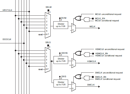
I have practical difficulties to rise SMCKL at 24MHz DCO on MSP432 rev.C to the ratio MCKL/SMCLK = 1:1. I've changed LDO to VCore1 and cleared all dividers. No result: SMCLK = 12 MHz, MCLK=24MHz.

    // Switches LDO to VCORE1
    while((PCM->CTL1 & PCM_CTL1_PMR_BUSY));
    PCM->CTL0 = PCM_CTL0_KEY_VAL | PCM_CTL0_AMR_1;
    while((PCM->CTL1 & PCM_CTL1_PMR_BUSY));

    CS->KEY = CS_KEY_VAL;
    CS->CTL0 = CS_CTL0_DCORSEL_4;    // Set DCO to 24MHz
    CS->CTL1 = (CS->CTL1 & ~(CS_CTL1_SELM_MASK | CS_CTL1_DIVM_MASK | CS_CTL1_DIVHS_MASK | CS_CTL1_DIVS_MASK | CS_CTL1_SELS_MASK)) | CS_CTL1_SELA__REFOCLK | CS_CTL1_SELS__DCOCLK | CS_CTL1_SELM__DCOCLK;
    CS->KEY = 0;

Any ideas why or how to solve it?

Alexey

  • Alexey,
    How are you verifying the clock frequency? I will see if I can reproduce.
    Thank you,
    Chris
  • I send some amount of data to external device through SPI driven by SMCLK without any delays. SPI is configured without dividers too. Then I measure amount of time spent on this event, which does not vary from mathematical recalculations.
    MSP432 does have peripheral bus restrictions, so it cannot work more that 12MHz at VCore0, and 24MHz at VCore1. So I've tried to fulfill such conditions and find any additional configuration registers how to disable such SMCLK restrictions. FLASH is driven by SMCKL, then at 24MHz DCO it is also working at 12MHz without any-wait states (as Rev.B). But TI claims that FLASH on MSP432 rev.C can work at 24MHz without any wait-states. So, is it some kind of trick by lowering SMCLK?

    Regards,
    Alexey

  • Alexey,

       Thank you.  I think there is some confusion over the main and sub-main clock systems.  I typically think of MCLK running the CPU, Flash, and DMA (also there is an instance where the MCLK can source the ADC).  SMCLK is used for peripherals like timers and communications.   For example in tables 5.6 and 5.8 of the datasheet you see the frequencies defined in terms of MCLK.   The peripheral ranges in table 5.7 are often (but not always) in the context of SMCLK.

       Again, I will continue to look into this.  Attached is the code example that I am working from.

    Regards,

    Chris

    msp432p401x_cs_03a.c
    /* --COPYRIGHT--,BSD_EX
     * Copyright (c) 2013, Texas Instruments Incorporated
     * All rights reserved.
     *
     * Redistribution and use in source and binary forms, with or without
     * modification, are permitted provided that the following conditions
     * are met:
     *
     * *  Redistributions of source code must retain the above copyright
     *    notice, this list of conditions and the following disclaimer.
     *
     * *  Redistributions in binary form must reproduce the above copyright
     *    notice, this list of conditions and the following disclaimer in the
     *    documentation and/or other materials provided with the distribution.
     *
     * *  Neither the name of Texas Instruments Incorporated nor the names of
     *    its contributors may be used to endorse or promote products derived
     *    from this software without specific prior written permission.
     *
     * THIS SOFTWARE IS PROVIDED BY THE COPYRIGHT HOLDERS AND CONTRIBUTORS "AS IS"
     * AND ANY EXPRESS OR IMPLIED WARRANTIES, INCLUDING, BUT NOT LIMITED TO,
     * THE IMPLIED WARRANTIES OF MERCHANTABILITY AND FITNESS FOR A PARTICULAR
     * PURPOSE ARE DISCLAIMED. IN NO EVENT SHALL THE COPYRIGHT OWNER OR
     * CONTRIBUTORS BE LIABLE FOR ANY DIRECT, INDIRECT, INCIDENTAL, SPECIAL,
     * EXEMPLARY, OR CONSEQUENTIAL DAMAGES (INCLUDING, BUT NOT LIMITED TO,
     * PROCUREMENT OF SUBSTITUTE GOODS OR SERVICES; LOSS OF USE, DATA, OR PROFITS;
     * OR BUSINESS INTERRUPTION) HOWEVER CAUSED AND ON ANY THEORY OF LIABILITY,
     * WHETHER IN CONTRACT, STRICT LIABILITY, OR TORT (INCLUDING NEGLIGENCE OR
     * OTHERWISE) ARISING IN ANY WAY OUT OF THE USE OF THIS SOFTWARE,
     * EVEN IF ADVISED OF THE POSSIBILITY OF SUCH DAMAGE.
     *
     *******************************************************************************
     *
     *                       MSP432 CODE EXAMPLE DISCLAIMER
     *
     * MSP432 code examples are self-contained low-level programs that typically
     * demonstrate a single peripheral function or device feature in a highly
     * concise manner. For this the code may rely on the device's power-on default
     * register values and settings such as the clock configuration and care must
     * be taken when combining code from several examples to avoid potential side
     * effects. Also see http://www.ti.com/tool/mspdriverlib for an API functional
     * library & https://dev.ti.com/pinmux/ for a GUI approach to peripheral configuration.
     *
     * --/COPYRIGHT--*/
    //******************************************************************************
    //   MSP432P401 Demo - Device configuration for operation @ MCLK = DCO = 48MHz
    //
    //   Description: Proper device configuration to enable operation at MCLK=48MHz
    //   including:
    //   1. Configure VCORE level to 1
    //   2. Configure flash wait-state to 1
    //   3. Configure DCO frequency to 48MHz
    //   4. Ensure MCLK is sourced by DCO
    //
    //   After configuration is complete, MCLK is output to port pin P4.3.
    //
    //                MSP432P401x
    //             -----------------
    //         /|\|                 |
    //          | |                 |
    //          --|RST              |
    //            |             P4.3|----> MCLK
    //            |                 |
    //
    //   William Goh
    //   Texas Instruments Inc.
    //   June 2016 (updated) | November 2013 (created)
    //   Built with CCSv6.1, IAR, Keil, GCC
    //******************************************************************************
    #include "msp.h"
    #include "stdint.h"
    
    
    void error(void);
    
    int main(void)
    {
        volatile uint32_t i;
        uint32_t currentPowerState;
    
        WDT_A->CTL = WDT_A_CTL_PW |
                     WDT_A_CTL_HOLD;            // Stop WDT
    
        P1->DIR |= BIT0;                        // P1.0 set as output
    
        /* NOTE: This example assumes the default power state is AM0_LDO.
         * Refer to  msp432p401x_pcm_0x code examples for more complete PCM
         * operations to exercise various power state transitions between active
         * modes.
         */
    
        /* Step 1: Transition to VCORE Level 1: AM0_LDO --> AM1_LDO */
    
        /* Get current power state, if it's not AM0_LDO, error out */
        currentPowerState = PCM->CTL0 & PCM_CTL0_CPM_MASK;
        if (currentPowerState != PCM_CTL0_CPM_0)
            error();
    
        while ((PCM->CTL1 & PCM_CTL1_PMR_BUSY));
        PCM->CTL0 = PCM_CTL0_KEY_VAL | PCM_CTL0_AMR_1;
        while ((PCM->CTL1 & PCM_CTL1_PMR_BUSY));
        if (PCM->IFG & PCM_IFG_AM_INVALID_TR_IFG)
            error();                            // Error if transition was not successful
        if ((PCM->CTL0 & PCM_CTL0_CPM_MASK) != PCM_CTL0_CPM_1)
            error();                            // Error if device is not in AM1_LDO mode
    
        /* Step 2: Configure Flash wait-state to 1 for both banks 0 & 1 */
        FLCTL->BANK0_RDCTL = (FLCTL->BANK0_RDCTL & ~(FLCTL_BANK0_RDCTL_WAIT_MASK)) |
                FLCTL_BANK0_RDCTL_WAIT_1;
        FLCTL->BANK1_RDCTL  = (FLCTL->BANK0_RDCTL & ~(FLCTL_BANK1_RDCTL_WAIT_MASK)) |
                FLCTL_BANK1_RDCTL_WAIT_1;
    
        /* Step 3: Configure DCO to 48MHz, ensure MCLK uses DCO as source*/
    //    CS->KEY = CS_KEY_VAL ;                  // Unlock CS module for register access
    //    CS->CTL0 = 0;                           // Reset tuning parameters
    //    CS->CTL0 = CS_CTL0_DCORSEL_5;           // Set DCO to 48MHz
    //    /* Select MCLK = DCO, no divider */
    //    CS->CTL1 = CS->CTL1 & ~(CS_CTL1_SELM_MASK | CS_CTL1_DIVM_MASK) |
    //            CS_CTL1_SELM_3;
    //    CS->KEY = 0; // Lock CS module from unintended accesses
    
        CS->KEY = CS_KEY_VAL;
    //    CS->CTL0 = 0;                           // Reset tuning parameters
        CS->CTL0 = CS_CTL0_DCORSEL_4;    // Set DCO to 24MHz
        CS->CTL1 = (CS->CTL1 & ~(CS_CTL1_SELM_MASK | CS_CTL1_DIVM_MASK |
        		CS_CTL1_DIVHS_MASK | CS_CTL1_DIVS_MASK | CS_CTL1_SELS_MASK)) |
        				CS_CTL1_SELA__REFOCLK | CS_CTL1_SELS__DCOCLK |
    					CS_CTL1_SELM__DCOCLK; // | CS_CTL1_DIVS__2 | CS_CTL1_DIVM__2;
        CS->KEY = 0;
    
        /* Step 4: Output MCLK to port pin to demonstrate 48MHz operation */
        P4->DIR |= BIT3;
        P4->SEL0 |=BIT3;                        // Output MCLK
        P4->SEL1 &= ~(BIT3);
    
        P7->DIR |= BIT0;
        P7->SEL0 |=BIT0;                        // Output SMCLK
        P7->SEL1 &= ~(BIT0);
    
        while (1)                               // continuous loop
        {
            P1->OUT ^= BIT0;                    // Blink P1.0 LED
            for (i = 200000; i > 0; i--);       // Delay
        }
    }
    
    void error(void)
    {
        volatile uint32_t i;
    
        while (1)
        {
            P1->OUT ^= BIT0;
            for(i = 20000; i > 0; i--);           // Blink LED forever
        }
    }
    

  • I found the answer about SMCKL:
    MSP432 Technical Reference Manual, s.5.1: "SMCLK is limited in frequency to half of the rated maximum frequency of HSMCLK.".
    And no information yet about FLASH clock routing.

    Alexey
  • HSMCLK maximum frequency is 48 MHz. So, the limitation to SMCLK is pointed about half of the maximum, - 24MHz. From such statement it is unclear: is it limited by using static 1/2 divider or it has some 'smart' adaptation (to Core voltage and DCO) or unlocking, accessible by clock system register, which I didn't find.

    Alexey
  • Chris Sterzik said:
     I typically think of MCLK running the CPU, Flash, and DMA

    Chris,

    Why in MSP432 LPM0 mode the CPU is off as MCLK source is off, but Flash and DMA is available?

    And in technical documentation there is nothing present like additional 1/2 clock divider between HSMCLK and SMCLK.

    Alexey

  • Alexey,
    I believe the TRM is incorrect/inconsistent when it states that the CPU clock is also turned off:
    1. section 1.7 states that sleep mode stops the processor clock
    2. table 7-1 describes LPM0 where CPU is inactive, DMA and FLASH are available

    I do believe that the MCLK could potentially turn off if no clock request is made through the MCLK conditional request logic.

    Specific to your question about the additional 1/2 clock divider, there is none. There are no safeguards within the clocking system to prevent the specification violation of selecting an SMCLK greater than 24Mhz.

    Back to your original query I have verified that 24Mhz is output on both MCLK and SMCLK, moreover, if you replace the while loop with a sleep command (LPM0) the outputs are still there because of the clock request logic ( digital IO is requesting both MCLK and SMCLK).

    Best Regards,
    Chris
  • I accept your answer. But this does not mean that I fully agree with it. It definitely has not resolved my issue. But thank you for your effort and explanation.
    I have no tools to measure 24MHz directly from the pins.
    Consider this issue closed.

    Regards,
    Alexey

**Attention** This is a public forum